Large-aperture optical element surface shape detection method based on stacked coherent diffraction imaging
A technology of coherent diffraction imaging and optical components, which is applied in the direction of using optical devices, measuring devices, image analysis, etc., can solve the problem of small measurement field of view, and achieve the effect of large field of view, simple measurement optical path, and extended measurement range.
- Summary
- Abstract
- Description
- Claims
- Application Information
AI Technical Summary
Problems solved by technology
Method used
Image
Examples
Embodiment 1
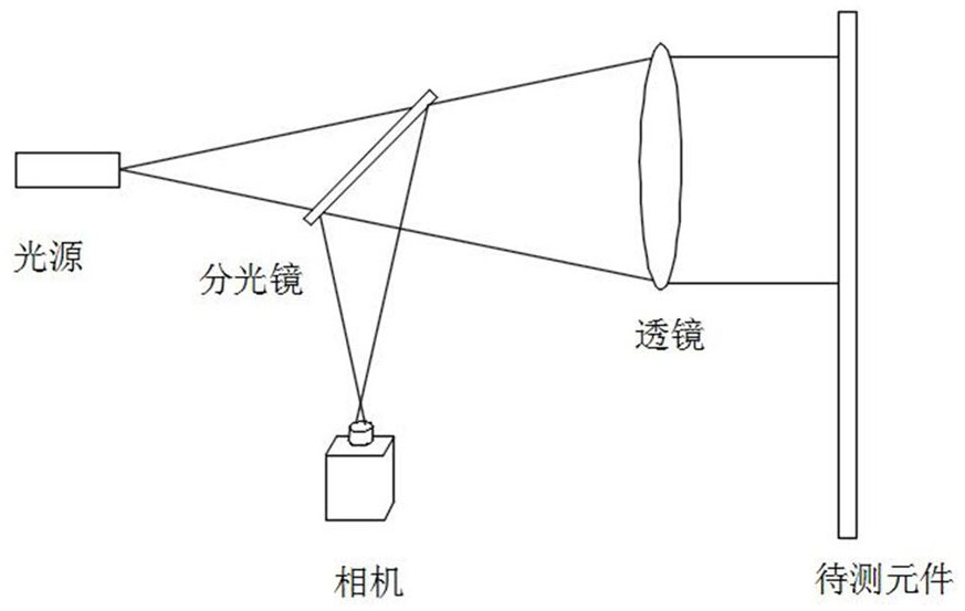
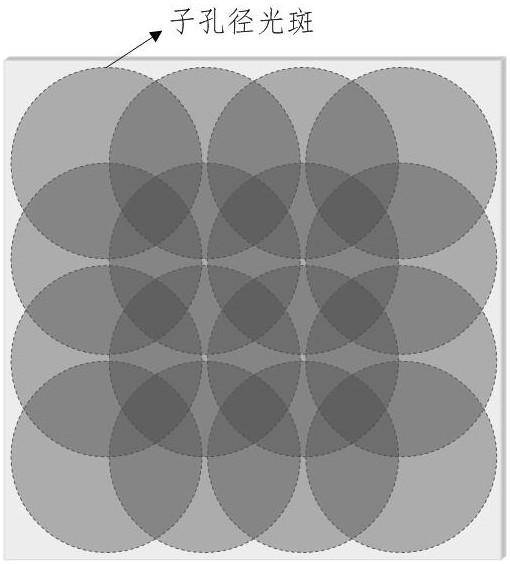
[0038] Such as figure 1 and figure 2 As shown, a large-aperture optical component surface shape detection method based on stacked coherent diffraction imaging, the component to be tested is located at the parallel light after beam expansion and collimation, and the parallel light aperture is limited by the collimator lens aperture. Considering the measurement efficiency, lens processing difficulty and cost factors, the general collimator lens diameter can be 100mm~200mm. Including the following steps:
[0039] Step 1. Move the component to be tested to the initial sub-aperture scanning position and align it, and use the camera to collect the diffraction spot image at the initial sub-aperture scanning position;
[0040] Step 2. Translate the component to be measured to the next sub-aperture scanning position and collect the diffraction spot image corresponding to the sub-aperture scanning position. Adjacent sub-apertures have overlapping areas, and the component to be measur...
Embodiment 2
[0060] This embodiment provides a method for automatically extracting the center of a cross figure based on least squares fitting iterations, the steps are as follows:
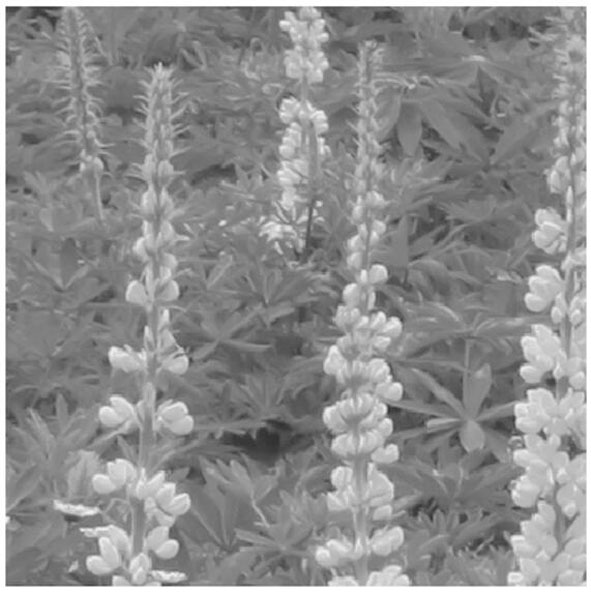
[0061] Step 1. Move the component to be tested to the initial scanning position and perform alignment; the surface shape distribution of the component to be tested simulated in this embodiment is as follows: image 3 As shown, the component size is 400mm×400mm, the component surface PV is 0.5λ (λ=632.8nm), and the measuring beam aperture is 100mm.
[0062] Step 2. Use a camera to collect the diffraction spot; the simulated camera in this embodiment has a pixel resolution of 1000×1000 and a pixel size of 5 μm.
[0063] Step 3. Translate the component to be tested to the next scanning position and collect the diffraction spot. The sub-apertures of adjacent scanning positions must have a certain overlapping area; the ratio of the area of the overlapping area to the area of the sub-aperture is 60%.
[0064] S...
PUM
 Abstract
Description
Claims
Application Information


