Trigger signal synchronization system and method based on delay chain, and semiconductor test equipment

A technology of trigger signal and synchronization system, applied in computer-aided design, special data processing applications, instruments, etc., to optimize the synchronization test of trigger signal, avoid unusable, and solve the effect of complicated backplane wiring

Active Publication Date: 2021-07-16
杭州加速科技有限公司
View PDF11 Cites 6 Cited by
  • Summary
  • Abstract
  • Description
  • Claims
  • Application Information

AI Technical Summary

Problems solved by technology

The trigger signal transmitted by the service board is processed by the programmable logic device, which solves the problem of synchronizing the trigger signal to multiple service boards

Method used


Image

  • Trigger signal synchronization system and method based on delay chain, and semiconductor test equipment
  • Trigger signal synchronization system and method based on delay chain, and semiconductor test equipment
  • Trigger signal synchronization system and method based on delay chain, and semiconductor test equipment

Examples


Embodiment 1

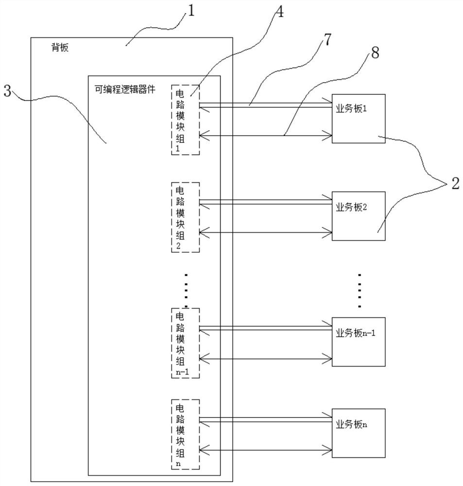
[0074] As attached to the manual figure 1 As shown, the trigger signal synchronization system based on the delay chain in a kind of ATE semiconductor test equipment provided by the present embodiment includes:

[0075] Backplane 1 and several service boards 2; service boards 2 are used to realize preset functions.

[0076] The backplane 1 is provided with a programmable logic device 3, and the programmable logic device 3 communicates with the service board 2 for receiving, processing and distributing the trigger signal with the service board 2, and the service board 2 transmits the trigger signal to the programmable The logic device 3, the programmable logic device 3 receives, processes and distributes the trigger signal transmitted by the service board 2.

[0077] In the programmable logic device 3 , the direction and transmission of signals can be realized through programming. Specifically, EDA tools can be used to perform equal-length layout and wiring to obtain the netli...

Embodiment 2

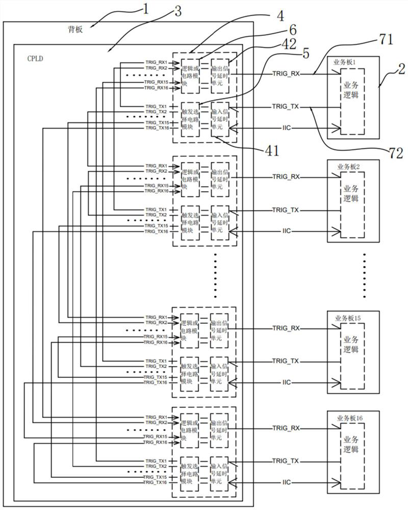
[0113] This embodiment also provides a trigger signal synchronization method for multi-service boards in ATE test equipment, which is used to synchronously select trigger signals between fan-out service boards 2, and is applicable to a system including a backplane and several service boards. The programmable logic device 3 communicates with each service board 2 . A programmable logic device is arranged on the backplane, and several circuit module groups are arranged inside the programmable logic device, and each circuit module group corresponds to each service board one by one and communicates with each other. The specific steps are attached in the manual Figure 9 As shown, the scheme is:

[0114] 101. Establish a communication connection between the backplane and each service board through a programmable logic device;

[0115] 102. Adjust the time for multiple circuit module groups to receive the trigger signal through the input signal delay unit 41, so as to realize that ...

Embodiment 3

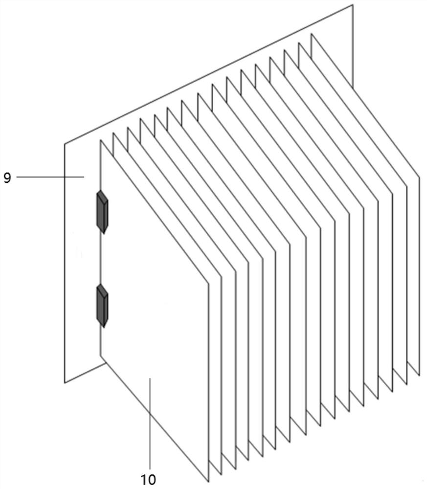
[0132] This embodiment also provides a kind of semiconductor test equipment, based on the trigger signal synchronization method based on the delay chain in the above-mentioned ATE semiconductor test equipment, such as image 3 shown, including:


PUM


Abstract

The invention discloses a trigger signal synchronization system and method based on a delay chain in ATE semiconductor test equipment and the semiconductor test equipment, and belongs to the field of integrated circuit test in the microelectronic industry. A programmable logic device is arranged on the backboard, interconnection synchronous trigger signal wiring of all service boards in communication connection with the backboard is achieved on the programmable logic device, and the problem that wiring of the backboard is numerous and jumbled is solved. An input signal delay unit and an output signal delay unit are arranged to perform delay processing on sending and receiving of the trigger signals, so that the problem of accurate synchronism of sending the trigger signals of each service board to other service boards is solved, and meanwhile, synchronous calibration processing of the trigger signals is easier.

Description

technical field [0001] The invention relates to the field of integrated circuit testing in the microelectronics industry, in particular to a trigger signal synchronization system and method based on delay chains in ATE semiconductor testing equipment and the semiconductor testing equipment. Background technique [0002] The backplane is a type of PCB (Printed Circuit Board). Specifically, a backplane is a motherboard that hosts daughterboards or line cards for custom functions. The main function of the backplane is to "carry" the board and distribute functions such as power, signals, etc. to each daughter board for proper electrical connection and signal transmission. The service board and the backplane work together, and the communication connection between the service board and the backplane, and the backplane can guide the logical operation of the entire system. [0003] At present, the wiring design of the backplane is difficult due to the large number of wires. Takin...

Claims


Application Information

Patent Timeline
Patent Type & Authority Applications(China)
IPC IPC(8): G06F30/347G06F30/333G06F13/42
CPCG06F30/347G06F30/333G06F13/4291
Inventor 邬刚陈永
Owner 杭州加速科技有限公司
Why Eureka
Try Eureka