CMOS ultra-wideband low-noise amplifier

A low-noise amplifier and ultra-wideband technology, which is applied in the direction of improving amplifiers to reduce noise effects, etc., to achieve good gain and reduce noise figure.

Pending Publication Date: 2021-07-16
GUILIN UNIV OF ELECTRONIC TECH
View PDF0 Cites 0 Cited by
  • Summary
  • Abstract
  • Description
  • Claims
  • Application Information

AI Technical Summary

Problems solved by technology

[0005] The present invention solves the problems of ultra-wideband, low noise and low power consumption in the background technology, and provides a CMOS ultra-wideband low-noise amplifier

Method used


Image

  • CMOS ultra-wideband low-noise amplifier
  • CMOS ultra-wideband low-noise amplifier
  • CMOS ultra-wideband low-noise amplifier

Examples


Embodiment Construction

[0021] In order to make the purpose, technical solution and advantages of the present invention clearer, the present invention will be further described in detail below in conjunction with the implementation modes and accompanying drawings.

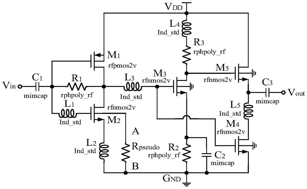
[0022] A CMOS ultra-wideband low-noise amplifier, such as figure 1 As shown, it adopts a single-ended input and output structure, and is composed of an input-stage complementary common-source circuit, an intermediate-stage common-source negative feedback circuit and an output-stage common-source buffer circuit. The input-stage complementary common-source circuit is connected to the intermediate-stage common-source negative feedback circuit, and the output end of the intermediate-stage common-source negative feedback circuit is connected to the output-stage common-source buffer circuit.

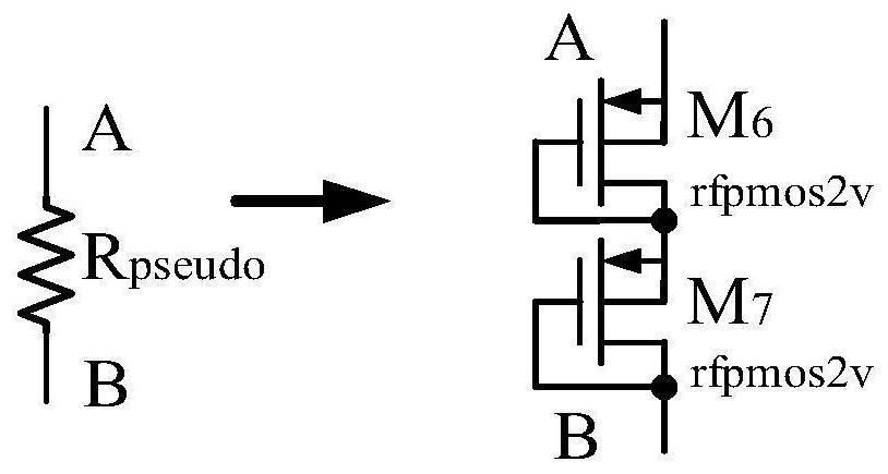
[0023] The input stage complementary common source circuit includes a PMOS transistor M1, an NMOS transistor M2, an input coupling capacitor C1, a feedba...


PUM


Abstract

The invention discloses a CMOS ultra-wideband low-noise amplifier which comprises an input-stage complementary common-source circuit, an intermediate-stage common-source negative feedback circuit and an output-stage common-source buffer circuit. Resistance feedback, an inductance peaking technology, a source electrode degeneration inductance technology and a pseudo resistance structure are innovatively introduced on the basis of a complementary common source electrode, and meanwhile, a common-source negative feedback circuit, a common-source buffer circuit and a current multiplexing technology are combined, so that the whole circuit has wide bandwidth, and meanwhile, good indexes such as gain, noise coefficient and power consumption are achieved. The antenna can work in a frequency band of 0.15-11 GHz, covers a 5G middle and low frequency band range (450 MHz to 6 GHz) and a 6GHz candidate frequency band range (5925-7125 MHz) of an IMT service, and is compatible with a UWB standard frequency band (3.1-10.6 GHz) at the same time.

Description

technical field [0001] The invention relates to the technical field of integrated circuit design, in particular to a CMOS ultra-wideband low-noise amplifier. Background technique [0002] With the rapid development of wireless technology, the development of mobile communication technology is developing towards higher frequency and wider bandwidth. Various wireless standards (such as Bluetooth, Zigbee, WLAN, WiFi, UWB, GPS and 2G / 3G / 4G / 5G cellular Telephone) use has been increasing. However, spectrum resources are limited. In order to meet people's communication needs for higher speed and larger capacity, ultra-wideband communication technology compatible with multiple communication standards has gradually become an important research direction. [0003] The ultra-wideband low-noise amplifier circuit is the core circuit module of the ultra-wideband receiver. As the first-stage amplifier circuit of the ultra-wideband receiving link, according to the noise cascading formula, t...

Claims


Application Information

Patent Timeline
Patent Type & Authority Applications(China)
IPC IPC(8): H03F1/26
CPCH03F1/26
Inventor 岳宏卫杨华光
Owner GUILIN UNIV OF ELECTRONIC TECH
Why Eureka
Try Eureka