

Groove type MOSFET device and preparation method thereof
A trench type, trench technology, applied in semiconductor/solid-state device manufacturing, semiconductor devices, electrical components, etc., can solve problems such as slow switching response, and achieve the effect of reducing connection paths, reducing resistance, and improving switching response.
- Summary
- Abstract
- Description
- Claims
- Application Information
AI Technical Summary
Problems solved by technology
Method used
Image

Examples
preparation example Construction
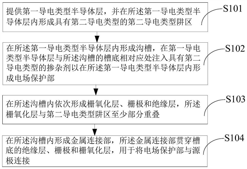
[0071] In addition, the present invention also provides a method for preparing a trench type MOSFET device, such as image 3 shown, including the following steps:
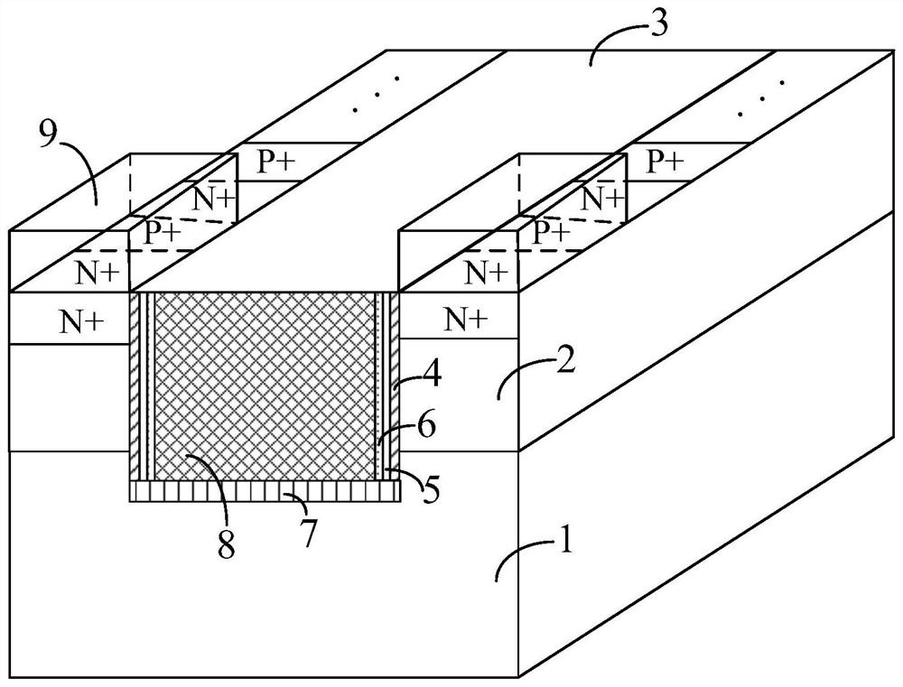
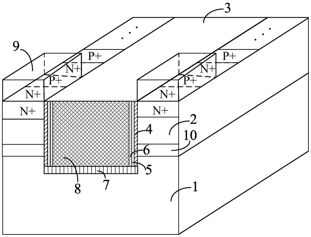
[0072] providing a first conductivity type semiconductor layer, and forming a second conductivity type well region having a second conductivity type in the first conductivity type semiconductor layer;
[0073] A trench is formed in the semiconductor layer of the first conductivity type, and a dopant of the second conductivity type is injected into the semiconductor layer of the first conductivity type corresponding to the groove bottom of the trench to form a dopant of the second conductivity type in the semiconductor layer of the first conductivity type. An electric field protection portion is formed in the semiconductor layer;
[0074] sequentially forming a gate oxide layer, a gate, and an insulating layer in the trench, the gate oxide layer at least partially overlapping the second conductivity type well regio...
Embodiment approach
[0076] In one implementation manner, the step of forming a second conductivity type well region having a second conductivity type in the first conductivity type semiconductor layer includes:
[0077] Implanting dopants with the second conductivity type into the semiconductor layer of the first conductivity type to form a semiconductor layer of the second conductivity type, and heavily doping the semiconductor layer with the first conductivity type at intervals agent and a dopant of the second conductivity type to form an ohmic contact region to form a well region of the second conductivity type.
[0078] In another embodiment, a second conductivity type semiconductor layer is first formed on the first conductivity type semiconductor layer, and the second conductivity type semiconductor layer is heavily doped with a dopant of the first conductivity type and a dopant of the second conductivity type at intervals. The dopant of the second conductivity type is used to form an ohmic...
PUM
 Abstract
Description
Claims
Application Information