Light-emitting diode epitaxial wafer and manufacturing method thereof

A technology of light-emitting diodes and manufacturing methods, which is applied in the direction of semiconductor devices, electrical components, circuits, etc., can solve the problems of large compressive stress of InGaN layer and GaN layer, affecting LED luminous efficiency, and internal quantum efficiency decline, so as to improve internal quantum efficiency , Prevent electron overflow, reduce blocking effect

Active Publication Date: 2022-05-13
HC SEMITEK SUZHOU
View PDF0 Cites 0 Cited by
  • Summary
  • Abstract
  • Description
  • Claims
  • Application Information

AI Technical Summary

Problems solved by technology

However, there is a large lattice mismatch between the InGaN layer and the GaN layer, resulting in a large compressive stress between the InGaN layer and the GaN layer
Compressive stress will generate a piezoelectric polarization electric field, which reduces the overlap of electron and hole wave functions, resulting in a decrease in internal quantum efficiency, thereby affecting LED luminous efficiency

Method used


Image

  • Light-emitting diode epitaxial wafer and manufacturing method thereof
  • Light-emitting diode epitaxial wafer and manufacturing method thereof
  • Light-emitting diode epitaxial wafer and manufacturing method thereof

Examples


Embodiment Construction

[0026] In order to make the purpose, technical solution and advantages of the present disclosure clearer, the implementation manners of the present disclosure will be further described in detail below in conjunction with the accompanying drawings.

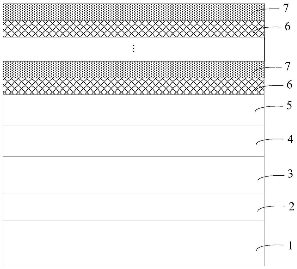
[0027] figure 1 is a schematic structural view of a light-emitting diode epitaxial wafer provided by an embodiment of the present disclosure, as shown in figure 1 As shown, the light-emitting diode epitaxial wafer includes a substrate 1 , and a low-temperature buffer layer 2 , a high-temperature buffer layer 3 , an N-type layer 4 and an active layer 5 sequentially stacked on the substrate 1 .

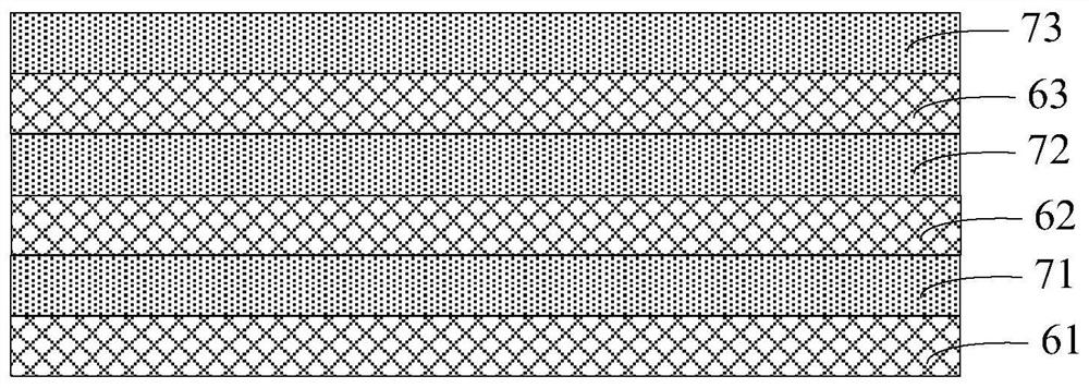
[0028] The light-emitting diode epitaxial wafer also includes a plurality of periodically alternately grown electron blocking layers 6 and P-type layers 7 stacked on the active layer 5 in sequence. Each electron blocking layer 6 is an AlGaN layer. Along the stacking direction of the epitaxial wafer, the Al composition in the electron blocki...


PUM

PropertyMeasurementUnit
thicknessaaaaaaaaaa
thicknessaaaaaaaaaa
thicknessaaaaaaaaaa

Abstract

The disclosure provides a light-emitting diode epitaxial wafer and a manufacturing method thereof, which belong to the technical field of semiconductors. The light-emitting diode epitaxial wafer includes a substrate, and a low-temperature buffer layer, a high-temperature buffer layer, an N-type layer and an active layer sequentially stacked on the substrate. A plurality of alternately grown electron blocking layers and P-type layers on the source layer, each of which is an AlGaN layer, along the stacking direction of the epitaxial wafer, in each period of the electron blocking layer The Al composition decreases gradually, the thickness decreases gradually, and the doping concentration of Mg in the P-type layer increases gradually in each period. The epitaxial wafer of the light emitting diode can increase the overlapping degree of the wave function of the electron and the hole in the spatial distribution, thereby improving the internal quantum efficiency of the LED.

Description

technical field [0001] The disclosure relates to the technical field of semiconductors, in particular to a light-emitting diode epitaxial wafer and a manufacturing method thereof. Background technique [0002] Light Emitting Diode (English: Light Emitting Diode, referred to as: LED) is a semiconductor electronic component that can emit light. As an efficient, environmentally friendly and green new solid-state lighting source, LED is a new generation of light source with broad prospects, and is being rapidly and widely used in traffic lights, car interior and exterior lights, urban landscape lighting, indoor and outdoor display screens and small-pitch displays. screen and other fields. [0003] Typically, GaN-based LEDs are epitaxially grown on sapphire substrates. The traditional GaN-based LED epitaxial structure generally adopts InGaN / GaN superlattice structure as the active layer. However, there is a large lattice mismatch between the InGaN layer and the GaN layer, resu...

Claims


Application Information

Patent Timeline
Patent Type & Authority Patents(China)
IPC IPC(8): H01L33/02H01L33/12H01L33/14H01L33/32H01L33/00
CPCH01L33/145H01L33/325H01L33/025H01L33/12H01L33/007
Inventor 姚振从颖董彬忠李鹏
Owner HC SEMITEK SUZHOU
Why Eureka
Try Eureka