Method for forming CIS sensor

A sensor and semiconductor technology, applied in the field of CIS sensor formation, can solve problems such as leakage and difficulties, and achieve the effect of preventing leakage

Inactive Publication Date: 2021-07-27
GUANGZHOU CANSEMI TECH INC
View PDF4 Cites 2 Cited by
  • Summary
  • Abstract
  • Description
  • Claims
  • Application Information

AI Technical Summary

Problems solved by technology

It is already very difficult to etch deep trench isolation structures (DTI) to a depth of 5um. When selecting an insulating region in the FEOL process, the IMP depth is limited by the thickness of the photoresist and the design rule, and cannot go deeper
There is a gap between the DTI and the insulating region, the lens 160 collects the light and transmits it to the filter 150, the red light filtered by the red filter 151 may generate electrons deep in the substrate 110, and the electrons may pass through the DTI and the insulating The gap between the areas enters the pixel area corresponding to the green light filter 152, resulting in leakage

Method used


Image

  • Method for forming CIS sensor
  • Method for forming CIS sensor
  • Method for forming CIS sensor

Examples


Embodiment Construction

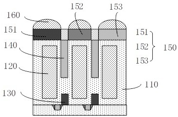
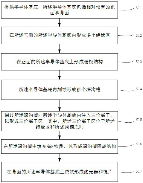
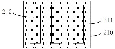
[0032] The specific implementation manner of the present invention will be described in more detail below with reference to schematic diagrams. The advantages and features of the present invention will be more apparent from the following description. It should be noted that all the drawings are in a very simplified form and use imprecise scales, and are only used to facilitate and clearly assist the purpose of illustrating the embodiments of the present invention.

[0033] Hereinafter, the terms "first", "second", etc. are used to distinguish between similar elements, and are not necessarily used to describe a specific order or chronological order. It is to be understood that these terms so used are interchangeable under appropriate circumstances. Similarly, if a method described herein includes a series of steps, the order in which these steps are presented is not necessarily the only order in which these steps can be performed, and some described steps may be omitted and / or...


PUM


Abstract

The invention provides a method for forming a CIS sensor, and the method comprises the steps: providing a semiconductor substrate which comprises a front surface and a back surface which are opposite to each other; forming a plurality of insulating regions in the semiconductor substrate on the front side; forming a gate structure on the semiconductor substrate on the front side; etching in the semiconductor substrate on the back surface to form a plurality of deep grooves; injecting trivalent ions into the semiconductor substrate through the deep trench to form a trivalent ion region, the trivalent ion region being located between the insulating region and the trench; filling the deep trench with a high-k substance to form a deep trench isolation structure; and sequentially forming an optical filter and a lens on the semiconductor substrate on the back surface. In the invention, the trivalent ion region can prevent electrons generated by light rays in the substrate from interfering with the adjacent photodiode region, so that the generation of electric leakage is prevented.

Description

technical field [0001] The invention relates to the technical field of semiconductors, in particular to a method for forming a CIS sensor. Background technique [0002] With the transfer of CIS (CMOS IMAGE SENSOR) sensor chips from front-illuminated (FSI) to back-illuminated (BSI) and stacked (stacked) technology, the market application scenarios of CIS are becoming wider and wider. The trend of CIS sensor chips is higher pixels and smaller pixels. The pixel size has been reduced from 1.75um FSI to 1.12um BSI, and even 0.8um BSI. [0003] As the size of the pixel (pixel) gradually decreases, the area isolated between the pixels (pixel) also shrinks synchronously, gradually shrinking from 0.5um to about 0.2um. At this time, the electrical crosstalk between pixels is very serious. Especially for red light with strong penetrating power, electron-hole pairs will still be excited in the deep region of the substrate, resulting in leakage. Even, the penetration of red light is a...

Claims


Application Information

Patent Timeline
Patent Type & Authority Applications(China)
IPC IPC(8): H01L27/146
CPCH01L27/1463H01L27/14683
Inventor 李玉科李振文石卓
Owner GUANGZHOU CANSEMI TECH INC
Why Eureka
Try Eureka