A kind of photoelectric glass with film circuit and production process

A photoelectric glass and production process technology, applied in glass/slag layered products, light sources, layered products, etc., can solve the problems of weakening lamp brightness, circuit damage, affecting visual effects, etc., to improve product yield, increase Service life, increase the effect of visual effects

Active Publication Date: 2021-11-26
合肥达视光电科技有限公司
View PDF0 Cites 0 Cited by
  • Summary
  • Abstract
  • Description
  • Claims
  • Application Information

AI Technical Summary

Problems solved by technology

[0004] (1) Since the circuit protrudes, it is easy to cause circuit damage during the pressing process and affect the yield;
[0005] (2) The circuit board inside the existing photoelectric glass is thicker and the light transmission is poor, which leads to not only complicated processing of the photoelectric glass in the production process, but also low transparency after the finished product, which affects the visual effect;
[0006] (3) The glass in the production process of photoelectric glass is relatively heavy, and the existing equipment is not enough to support the increased lamination work, resulting in a small size of photoelectric glass, which limits the scope of application of the product;
[0007] (4) The distance between the lamp beads in the existing photoelectric glass is large, and the picture imaging is poor, and the farther away from the power supply input end, the brightness of the lamp beads behind will gradually weaken, and the brightness is inconsistent, which affects the visual effect

Method used


Image

  • A kind of photoelectric glass with film circuit and production process
  • A kind of photoelectric glass with film circuit and production process
  • A kind of photoelectric glass with film circuit and production process

Examples


Embodiment 1

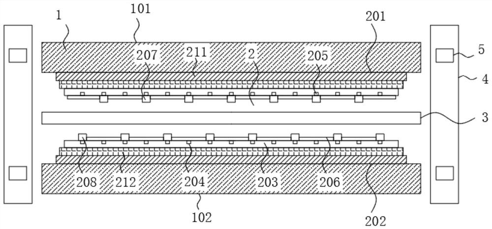
[0038] The invention provides a kind of photoelectric glass with a film line, such as Figure 1-3As shown, the photoelectric layer 2 is located inside the glass layer 1. By encapsulating the photoelectric glass with a film circuit, it is beneficial to encapsulate the photoelectric glass according to the ultra-thin and high transparency effect of the film circuit. The packaging process is relatively simple, which solves the traditional low-efficiency process methods such as direct laser engraving or printing on glass, saves costs, reduces energy consumption in the production process, improves product yield, and is not easy to damage the film line, and the finished product has a good visual effect;

[0039] The glass layer 1 includes an upper glass layer 101 and a lower glass layer 102, the photoelectric layer 2 includes a first conductive layer 201 and a second conductive layer 202, and the first conductive layer 201 is fixedly connected to the upper surface of the lower glass l...

Embodiment 2

[0042] The invention provides a kind of photoelectric glass with a film line, such as Figure 1-3 As shown, the photoelectric layer 2 is located inside the glass layer 1. By encapsulating the photoelectric glass with a film circuit, it is beneficial to encapsulate the photoelectric glass according to the ultra-thin and high transparency effect of the film circuit. The packaging process is relatively simple, which solves the traditional low-efficiency process methods such as direct laser engraving or printing on glass, saves costs, reduces energy consumption in the production process, improves product yield, and is not easy to damage the film line, and the finished product has a good visual effect;

[0043] The glass layer 1 includes an upper glass layer 101 and a lower glass layer 102, the photoelectric layer 2 includes a first conductive layer 201 and a second conductive layer 202, and the first conductive layer 201 is fixedly connected to the upper surface of the lower glass ...

Embodiment 3

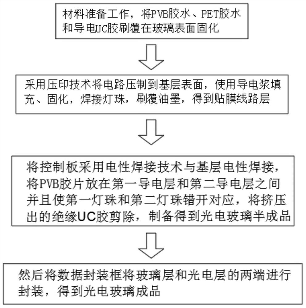
[0046] The invention also discloses a production process of photoelectric glass with a film-attached circuit, which includes the following steps:

[0047] S1: First, brush PVB glue and PET glue on the surface of the upper glass layer 101 and the lower glass layer 102 to form a transparent PVB glue layer 212 and a transparent PET layer 211, and then coat a layer of conductive UC glue on the surface of the transparent PET layer 211 and solidify Form the base layer 203 with high flatness, then engrave the circuit diagram to be embossed on the surface of the mold, and make the engraved circuit diagram appear as a raised display, and then emboss on the surface of the base layer 203 to emboss the circuit pattern to form an embossing groove 204, filling the prepared conductive paste into the circuit pattern in the embossing groove 204, scraping off the excess conductive paste, and drying to form the circuit layer 205;

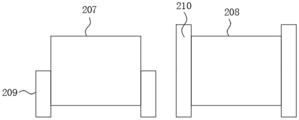
[0048] S2: Solder the first soldering layer 209 of the first lam...


PUM

PropertyMeasurementUnit
sizeaaaaaaaaaa
thicknessaaaaaaaaaa
thicknessaaaaaaaaaa

Abstract

The invention discloses a photoelectric glass with a film-attached circuit and a production process, comprising a glass layer and a photoelectric layer, the photoelectric layer is located inside the glass layer; the glass layer includes an upper glass layer and a lower glass layer, and the photoelectric layer It includes a first conductive layer and a second conductive layer, the first conductive layer is fixedly connected to the upper surface of the lower glass layer, and the second conductive layer is fixedly connected to the bottom wall of the upper glass layer. The present invention adopts the film-attached circuit for encapsulation in the photoelectric glass, effectively according to the ultra-thin and high-transparency effect of the film-attached circuit, which is beneficial to the photoelectric glass. Low-efficiency techniques such as engraving or printing save costs, reduce energy consumption in the production process, improve product yield, and are not easy to damage the film line, and the finished product has a good visual effect.

Description

technical field [0001] The invention belongs to the technical field of photoelectric glass production, and in particular relates to a photoelectric glass with a film-attached circuit and a production process. Background technique [0002] With the rapid development of the market economy, the market publicity platform has been continuously upgraded and transformed, people's concept of consumption has been continuously improved, and their tastes have gradually increased. From the traditional black display to the transparent display, from the past black display with high energy consumption and small size The bulky, unstable security and its low-end display effects have changed rapidly to the energy-saving and environmentally friendly, light and small, high-stability, high-end and novel display screens of transparent displays. After the traditional black display screen has high energy consumption, bulky size, unstable security, and the low-end display effect has shifted to the r...

Claims


Application Information

Patent Timeline
Patent Type & Authority Patents(China)
IPC IPC(8): B32B17/06B32B27/06B32B27/30B32B27/36B32B33/00B32B7/12B32B3/08F21V33/00F21V19/00F21Y115/10
CPCB32B3/085B32B7/12B32B17/06B32B27/06B32B27/30B32B27/36B32B33/00B32B2307/202F21V19/0025F21V33/00F21Y2115/10
Inventor 曹海波
Owner 合肥达视光电科技有限公司
Why Eureka
Try Eureka