Level shift circuit suitable for GaN half-bridge gate driving

A technology of level shifting circuit and gate drive, applied in logic circuit coupling/interface, logic circuit, high-efficiency power electronic conversion using field effect transistors, etc. It can solve system failure, false shutdown, GaN power tube false opening, etc. question

Active Publication Date: 2021-07-30
UNIV OF ELECTRONICS SCI & TECH OF CHINA
View PDF10 Cites 1 Cited by
  • Summary
  • Abstract
  • Description
  • Claims
  • Application Information

AI Technical Summary

Problems solved by technology

When the dV/dt of the switching node is high, the IP is large, and the undershoot and overshoot will touch the flipping thr

Method used


Image

  • Level shift circuit suitable for GaN half-bridge gate driving
  • Level shift circuit suitable for GaN half-bridge gate driving
  • Level shift circuit suitable for GaN half-bridge gate driving

Examples


Embodiment Construction

[0031] Below in conjunction with accompanying drawing, technical solution of the present invention is described in detail:

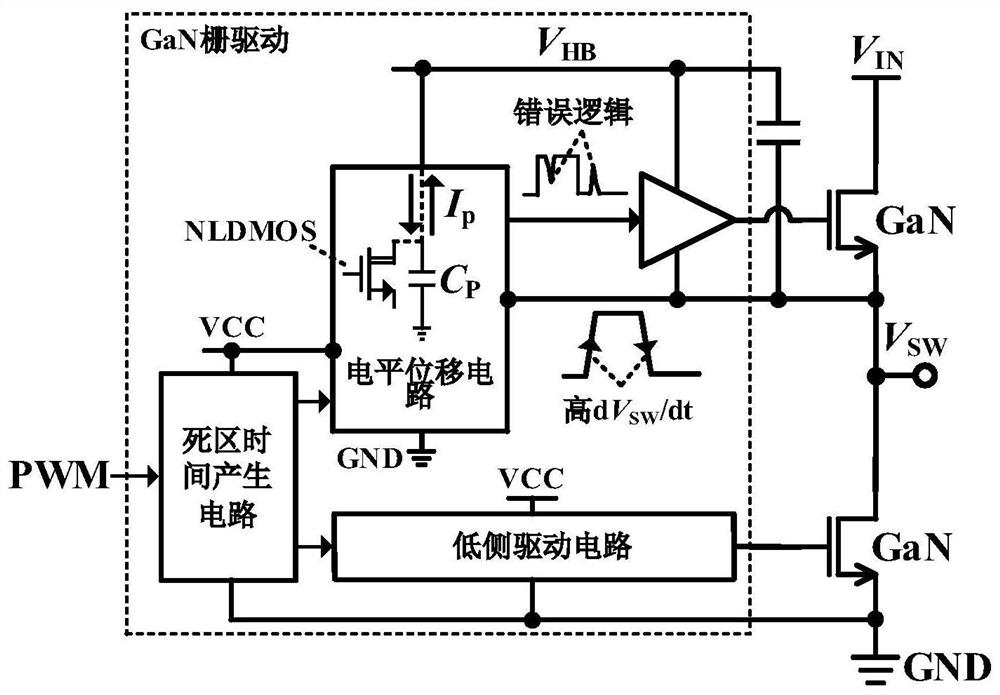
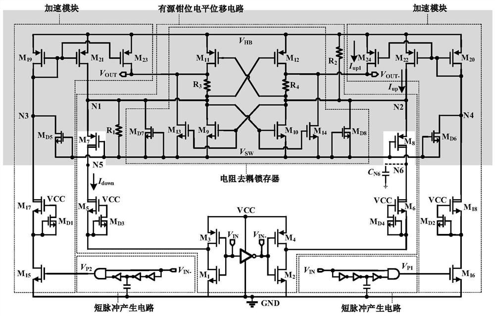
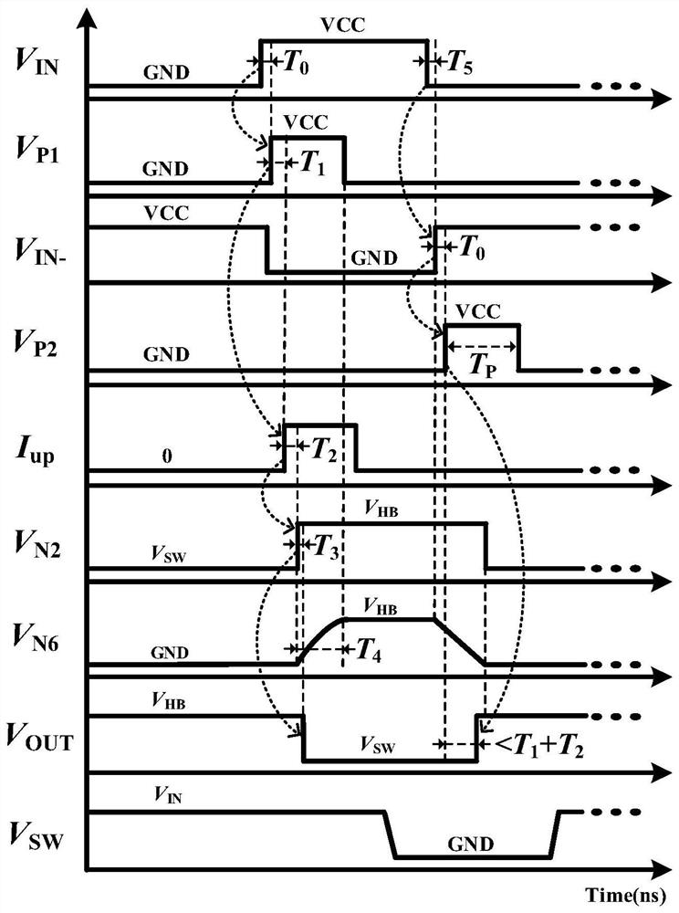
[0032] figure 2 Shown is the circuit structure of the level shift circuit of the present invention. The circuit is composed of three parts: an active clamp level shift circuit, an acceleration module and a short pulse generation circuit. Active-clamp level-shifting circuits incorporate resistively decoupled latches. The resistor decoupling latch and the acceleration module constitute a decoupling acceleration circuit.

[0033] In the resistive decoupling latch, a resistor is used to separate the PLDMOS source terminal with relatively large parasitic capacitance from the output terminal, blocking the high-side floating power supply ground V SW The effect on the output logic state of parasitic currents induced when dV / dt transitions occur. The acceleration module charges and discharges the parasitic capacitance relative to ground in the active clamp l...


PUM


Abstract

The invention belongs to the technical field of power supplies, and particularly relates to a level shift circuit suitable for GaN half-bridge gate driving. According to the level shift circuit provided by the invention, through the synergistic effect of the active clamping level shift circuit controlled by a PWM signal and the acceleration module controlled by the short pulse, the limitation of a large voltage dynamic range on an LDMOS parasitic capacitor on the speed is effectively avoided, and high-speed level conversion is realized. Meanwhile, nodes with relatively low stray capacitance in the circuit are separated from the output through the decoupling acceleration circuit, logic error overturning caused by charging and discharging of the stray capacitance opposite to the ground is effectively avoided in the dV/dt conversion process, and the dV/dt noise suppression capability is improved.

Description

technical field [0001] The invention belongs to the technical field of power supplies, and in particular relates to a level shift circuit suitable for GaN half-bridge gate driving. Background technique [0002] GaN power devices have smaller on-resistance and parasitic capacitance than Si MOSFET power devices, and have been considered as a good solution for miniaturizing power systems. As the core module in the GaN half-bridge gate drive circuit, the speed of the level shift circuit and the ability to resist the dV / dt interference of the floating power supply rail directly determine the operating frequency and reliability of the GaN half-bridge gate drive circuit. GaN gate drive circuits generally have a switching frequency as high as several MHz to tens of MHz, which makes the transmission delay of the GaN gate drive circuit as low as ten nanoseconds. Due to the extremely low parasitic capacitance of GaN power devices, the switching speed of GaN half-bridge switching nodes...

Claims


Application Information

Patent Timeline
IPC IPC(8): H03K19/0185
CPCH03K19/018557Y02B70/10
Inventor 明鑫秦尧刘媛媛孙天一王卓张波
Owner UNIV OF ELECTRONICS SCI & TECH OF CHINA
Why Eureka
Try Eureka