Manufacturing method of electronic product shell

A technology of electronic products and manufacturing methods, which is applied in the field of manufacturing electronic product shells, and can solve the problems of high tensile strength, complex structure bonding, easy delamination at the corner bonding position of the shell, investment in bubble bonding equipment, etc. problems, to achieve the effect of improving product environmental protection and weather resistance testing, ensuring material delivery, and enriching structures

Pending Publication Date: 2021-08-03
曹祖铭
View PDF2 Cites 1 Cited by
  • Summary
  • Abstract
  • Description
  • Claims
  • Application Information

AI Technical Summary

Problems solved by technology

[0003] One of the purposes of the present invention is to address the above-mentioned shortcomings and provide a method for manufacturing the casing of an electronic product, in order to solve the problem that similar processes in the prior art cannot satisfy high-stretch and complex structure bonding, and the corner bonding position of the casing is prone to appear. Technical issues such as delamination, wrinkling, rebound, and air bubbles, and cost issues such as high investment in laminating equipment, complicated processes, and low product yield

Method used


Image

  • Manufacturing method of electronic product shell

Examples


Embodiment Construction

[0028] The present invention will be further elaborated below in conjunction with specific examples.

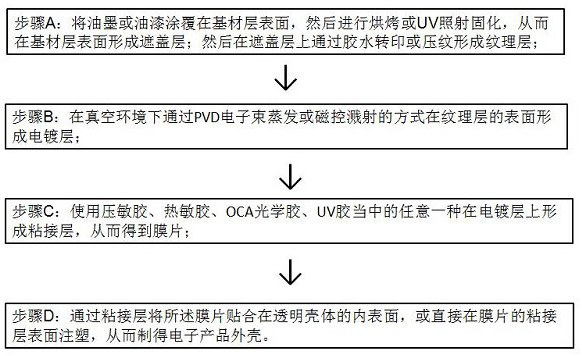
[0029] One embodiment of the present invention is a kind of manufacturing method of electronic product shell, and the concrete steps of this method making electronic product shell are:

[0030] Step 1. Coat one side of the base material with a release layer or make a cover layer that can adjust the adhesion to the base material. Spraying, lithographic printing, gravure printing, letterpress printing, digital printing, inkjet printing, dip-dyeing, coating, covering material transfer, any one or more superimposed methods to form a covering layer, if no release layer is made, directly It is enough to make a covering layer on the substrate layer by the aforementioned method, and if the non-peelable substrate uses a self-colored substrate, the covering layer does not need to be prepared.

[0031] Step 2, and then make a texture layer on the cover layer by UV transfer printing or ...


PUM


Abstract

The invention discloses a manufacturing method of an electronic product shell. The processed shell comprises a transparent shell and a diaphragm. The manufacturing method comprises the following specific steps: firstly, manufacturing the diaphragm of a release base material; then manufacturing the transparent shell through procedures such as injection molding, hot bending of glass or a composite board, pouring and the like; then attaching the transparent shell to the manufactured release diaphragm; and finally, conducting CNC carving on an attached product, wherein the base material can be selectively reserved or peeled off according to requirements on product characteristics. The method has no requirement on the optical property of the base material, so the base material is not limited by import, problems in material supply can be solved, and cost is greatly reduced; according to the method, the low-temperature thermal-deformation high-stretching base material is selected, so the problems of high stretching, complicated structure, crinkling, bubbles, layering, springback and the like during lamination are solved; and in addition, the middle layer of the diaphragm manufactured by the method is free of a base material, so the transmittance of the product can be directly improved by 7%-9% on an original basis, and an outer shell product is more transparent and more full and dazzling in color and texture.

Description

technical field [0001] The invention relates to a method for manufacturing an electronic product casing, and more specifically, the invention mainly relates to a method for manufacturing an electronic product casing. Background technique [0002] At present, the shells on electronic products, especially the common mobile phone back shells, mainly use PET material as the base material of the diaphragm, and then attach the diaphragm with color, pattern and texture to the transparent case, using OCA optical glue lamination process Make electronics enclosures. The casing of electronic products formed by the aforementioned bonding process needs to be bent directly before bonding the diaphragm, but the existing process cannot use heating methods to heat the PET sheet to the softening point for stretching and bonding (due to OCA optical The temperature resistance of the glue is 90°C, while the softening temperature of the PET material is about 150°C), and the existing bonding proc...

Claims


Application Information

Patent Timeline
IPC IPC(8): B32B27/06B32B27/36B32B27/40B32B33/00B32B7/06B32B7/12B32B38/00H05K5/02
CPCB32B27/06B32B27/36B32B27/40B32B33/00B32B7/06B32B7/12B32B38/145B32B38/164H05K5/0217B29C63/02Y02A30/00B29C45/14639H05K5/0017B29C45/14688C09J7/40C09D5/00C09D11/30C09D11/02C23C14/0015C23C14/30C23C14/35C03B23/006B29C2045/0079B32B37/12B32B2457/00
Inventor 曹祖铭
Owner 曹祖铭
Why Eureka
Try Eureka