A kind of nano silver solder paste low temperature large area uniform sintering method

A nano-silver, large-area technology, used in semiconductor devices, electrical components, circuits, etc., can solve the problems of high sintering temperature, higher sintering uniformity requirements, and inability to achieve, to improve sintering uniformity and avoid low connection strength. , the effect of improving the wetting ability

Active Publication Date: 2022-07-08
TIANJIN POLYTECHNIC UNIV
View PDF4 Cites 0 Cited by
  • Summary
  • Abstract
  • Description
  • Claims
  • Application Information

AI Technical Summary

Problems solved by technology

However, when using nano-silver solder paste to sinter and connect chips in the prior art, the sintering temperature is relatively high, and it usually needs to be kept at a sintering temperature of 250-300°C for a long time. withstand such high temperatures
In addition, the power chip area connected by the prior art is usually less than 150mm 2 , while the CPU chip in the integrated circuit generally has an area of ​​200-1000mm 2 , the connection area is larger, and the requirements for sintering uniformity are higher
The prior art method cannot realize sintering nano-silver solder paste at a lower temperature and the connection area is 200-1000mm 2 large area chip

Method used


Image

  • A kind of nano silver solder paste low temperature large area uniform sintering method
  • A kind of nano silver solder paste low temperature large area uniform sintering method
  • A kind of nano silver solder paste low temperature large area uniform sintering method

Examples


Embodiment 1

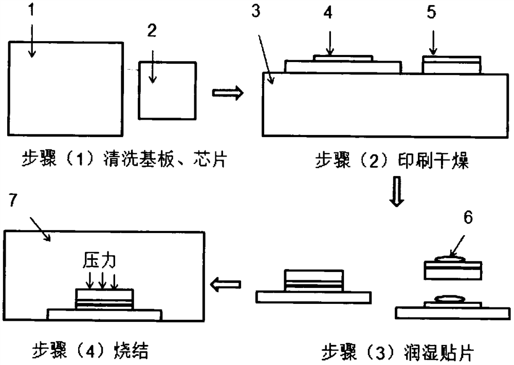
[0039] In this example, the process method for uniform sintering of nano-silver solder paste at low temperature and large area is as follows:

[0040] (1) Set the area to 400mm 2 The chips and metal substrates were ultrasonically cleaned in absolute ethanol for 1 min to remove the oily dirt adhering to the surface of the metal substrates, and then dried at 50°C for 1 min using a hot air blower to fully volatilize the absolute ethanol and water on the surfaces of the substrates and chips.

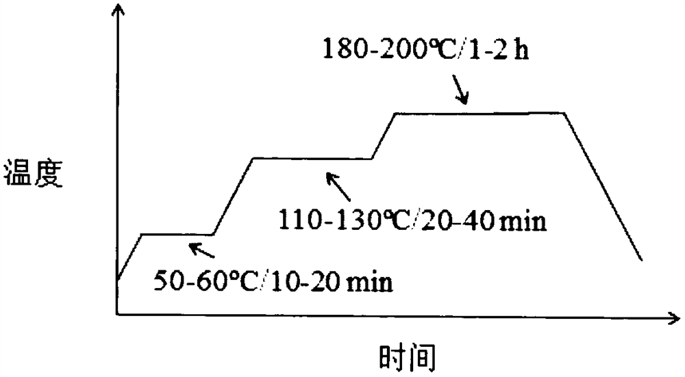
[0041] (2) Print 50 μm thick nano-silver solder paste on the substrate and chip connection surfaces cleaned in step (1), place the printed solder paste substrate and chip on a heating table and heat to 110°C for 20 minutes to dry to make the solder paste The low-temperature solvent and adhesive in the medium are fully decomposed and volatilized. After drying, the substrate and chip are removed and cooled to room temperature quickly.

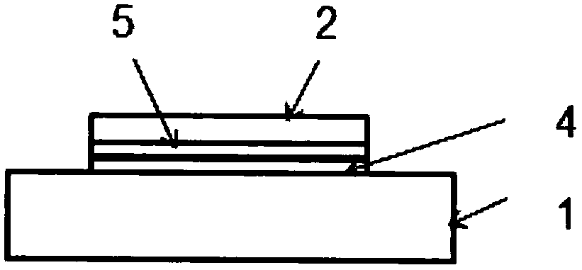
[0042] (3) drop an organic solvent on the nano-silver so...

Embodiment 2

[0045] In this example, the process method for uniform sintering of nano-silver solder paste at low temperature and large area is as follows:

[0046] (1) Set the area to 400mm 2 The chips and metal substrates were ultrasonically cleaned in absolute ethanol for 1.5 minutes to remove the oily dirt adhering to the surface of the metal substrates, and then dried at 75°C for 1.5 minutes using a hot air blower to fully volatilize the absolute ethanol and water on the surfaces of the substrates and chips. .

[0047] (2) Print 100μm thick nano-silver solder paste on the substrate and chip connection surfaces cleaned in step (1), place the printed solder paste substrate and chip on a heating table and heat to 120°C for 30 minutes to dry to make the solder paste The low-temperature solvent and adhesive in the medium are fully decomposed and volatilized. After drying, the substrate and chip are removed and cooled to room temperature quickly.

[0048] (3) drop an organic solvent on the...

Embodiment 3

[0051] In this example, the process method for uniform sintering of nano-silver solder paste at low temperature and large area is as follows:

[0052] (1) Set the area to 400mm 2 The chips and metal substrates were ultrasonically cleaned in absolute ethanol for 2 minutes to remove the oily dirt adhering to the surface of the metal substrates, and then dried at 100 °C for 2 minutes using a hot air blower to fully volatilize the absolute ethanol and water on the surfaces of the substrates and chips.

[0053] (2) Print 150 μm thick nano-silver solder paste on the substrate and chip connection surfaces cleaned in step (1), place the printed solder paste substrate and chip on a heating table and heat to 130°C for 40 minutes to dry to make the solder paste The low-temperature solvent and adhesive in the medium are fully decomposed and volatilized. After drying, the substrate and chip are removed and cooled to room temperature quickly.

[0054] (3) drop an organic solvent on the nan...


PUM

PropertyMeasurementUnit
thicknessaaaaaaaaaa
areaaaaaaaaaaa
thicknessaaaaaaaaaa

Abstract

The invention provides a method for uniform sintering of nano-silver solder paste at low temperature and large area. (3) drop an organic solvent on the nano silver solder paste on the surface of the substrate and chip after drying, wet the surface solder paste and patch; (4) place the substrate and chip on the wet patch in a sintering furnace, Pressure sintering at a low temperature of 180 ° C. By adopting the above technical solutions, the nano-silver solder paste can be uniformly sintered at a low temperature of 180-200°C with a connection area of ​​200-1000mm 2 of large-area chips. The low sintering temperature avoids the possible damage to the circuit board and chip casing caused by high temperature, while the residual stress of the sintered joint is smaller, and the heat-resistance-mechanical cycle capability is improved. Using the process of printing and drying first and then wetting the patch, the connection layer after sintering is uniform, and there is no air channel delamination defect, which improves the thermal conductivity and reliability of the large-area sintered silver layer.

Description

technical field [0001] The invention belongs to the field of power electronic device packaging, and in particular relates to a large-area semiconductor device connection method with high power and high reliability. Background technique [0002] In recent years, China's communication technology has developed rapidly. 5G network technology has progressed rapidly, and the communication rate has been greatly improved. At the same time, the chip integration has been further improved, and the chip area has continued to increase. Therefore, the power of the chip has risen sharply, the heat generation of the chip has increased seriously, and more and more manufacturers have realized the importance of packaging heat dissipation. The chip connection materials currently used in the field of integrated circuits are mainly low-temperature Sn-based solders with a melting point of 130-200° C., such as SnPb, SnBi, SnIn, and the like. However, the traditional low-temperature Sn-based solder...

Claims


Application Information

Patent Timeline
Patent Type & Authority Patents(China)
IPC IPC(8): H01L21/56H01L21/58H01L21/60
CPCH01L21/56H01L24/03H01L24/07
Inventor 梅云辉邓文斌
Owner TIANJIN POLYTECHNIC UNIV
Why Eureka
Try Eureka