Check patentability & draft patents in minutes with Patsnap Eureka AI!

Wafer semiconductor product, mask and photoetching machine

A semiconductor and mask technology, applied in the field of chip manufacturing technology, can solve the problems of increasing cost, reducing the number of dies, increasing the width of scribing lanes, etc., and achieving the effects of cost saving, increasing quantity, and reducing width

Pending Publication Date: 2021-08-06
北海惠科半导体科技有限公司
View PDF7 Cites 0 Cited by
  • Summary
  • Abstract
  • Description
  • Claims
  • Application Information

AI Technical Summary

Problems solved by technology

[0004] Although the above-mentioned die layout structure in the prior art can realize the alignment between the wafer and the mask plate, because it needs to increase the width of the scribing lane, it causes a waste of the wafer area, resulting in a decrease in the number of dies generated. reduction, increased cost

Method used


Image

  • Wafer semiconductor product, mask and photoetching machine
  • Wafer semiconductor product, mask and photoetching machine
  • Wafer semiconductor product, mask and photoetching machine

Examples


Embodiment Construction

[0033] Embodiments of the present invention are described in detail below, examples of which are shown in the drawings, wherein the same or similar reference numerals designate the same or similar elements or elements having the same or similar functions throughout. The embodiments described below by referring to the figures are exemplary and are intended to explain the present invention and should not be construed as limiting the present invention.

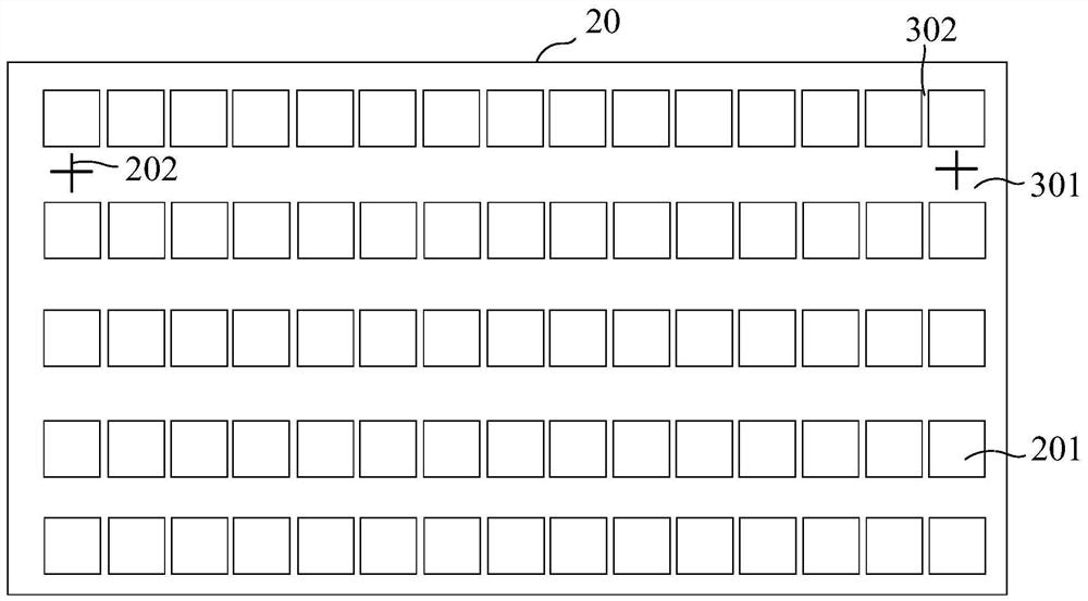
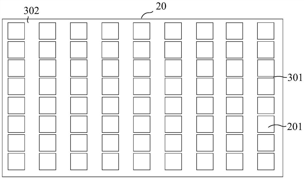
[0034] The invention provides a wafer semiconductor product. Compared with traditional wafer semiconductor products, the wafer semiconductor product can increase the number of dies under the same wafer area, thereby improving die production efficiency and reducing costs.

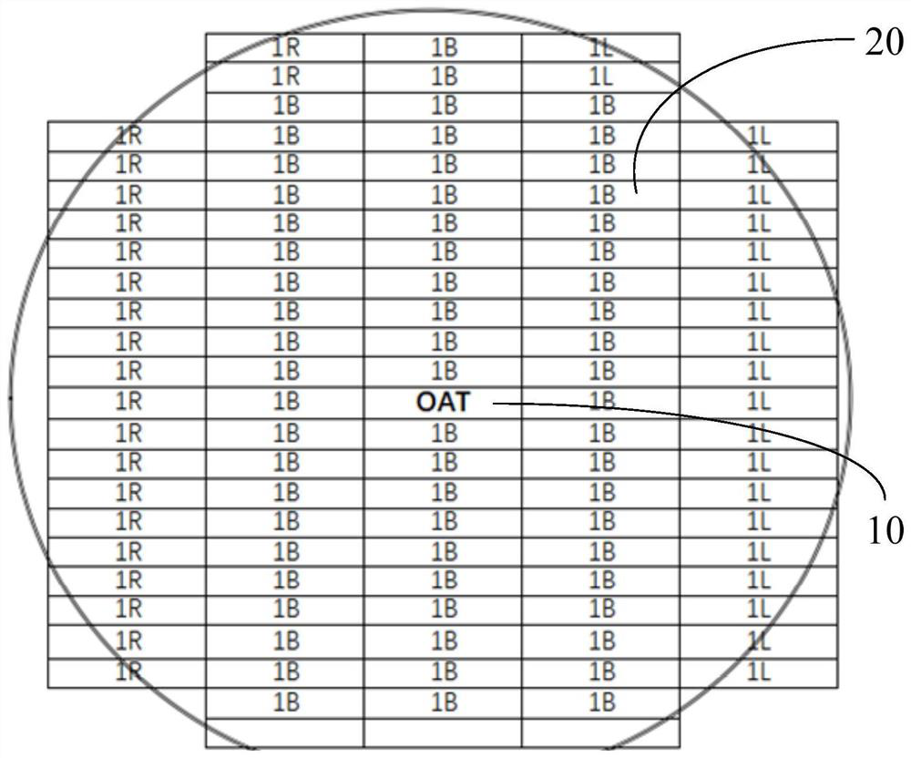
[0035] figure 1 It is a structural schematic diagram of an optical alignment field and a die exposure field of a wafer semiconductor product according to an embodiment of the present invention, and the wafer semiconductor product includes an optical alignment f...


PUM


Abstract

The invention provides a wafer semiconductor product, a mask and a photoetching machine. The wafer semiconductor product comprises a plurality of tube core exposure fields arranged on the wafer semiconductor product in a dot matrix mode, each tube core exposure field comprises a plurality of tube cores, a plurality of first scribing channels, a plurality of second scribing channels and at least one fine alignment target mark; the plurality of tube cores are arranged in a dot-matrix mode; the first scribing channels are formed between every two adjacent rows of tube cores; the second scribing channels are formed between every two adjacent columns of tube cores; and the fine alignment target mark and the plurality of tube cores are arranged in a non-overlapping mode; and the width of the fine alignment target mark is greater than that of the first scribing channels or the second scribing channels. According to the wafer semiconductor product, the fine alignment target mark is arranged in the area occupied by the tube cores, so that the width of the scribing channels can be reduced under the condition of ensuring alignment, the number of effective tube cores in the tube core exposure fields is further increased, and the cost is saved.

Description

technical field [0001] The invention relates to the technical field of chip manufacturing technology, in particular to a wafer semiconductor product, a mask plate and a photolithography machine. Background technique [0002] Before the chip lithography process of the Ultratech Stepper lithography machine (stepper lithography machine), it is necessary to align the lithography machine with the wafer. The approximate alignment steps are: first, the manipulator rotates the wafer on the wafer on the workbench, align the wafer with the wafer workbench, use the first mask, and perform optical alignment through the Optical Alignment Target Mark (OAT mark) on the first mask (referred to as OAT alignment). The corresponding position on the wafer semiconductor product is an optical alignment field (OAT field), and there are usually two or more OAT fields on a wafer semiconductor product. After the OAT alignment is performed by the calibration system of the lithography machine, a roug...

Claims


Application Information

Patent Timeline
IPC IPC(8): G03F9/00
CPCG03F9/7084G03F9/7076Y02P70/50
Inventor 潘钙王国峰杨忠武
Owner 北海惠科半导体科技有限公司
Features
  • R&D
  • Intellectual Property
  • Life Sciences
  • Materials
  • Tech Scout
  • Unparalleled Data Quality
  • Higher Quality Content
  • 60% Fewer Hallucinations
Learn More