Process for producing semiconductor bodies with MOVPE-layer sequence

A technology of semiconductor and layer sequence, applied in the direction of semiconductor devices, semiconductor/solid-state device manufacturing, electrical components, etc., can solve the problem of low external quantum efficiency, achieve the effect of improving light output coupling and improving light efficiency

Inactive Publication Date: 2003-12-24
SIEMENS AG
View PDF3 Cites 2 Cited by
  • Summary
  • Abstract
  • Description
  • Claims
  • Application Information

AI Technical Summary

Problems solved by technology

However, the external quantum efficiency of such diodes is still very low.

Method used


Image

  • Process for producing semiconductor bodies with MOVPE-layer sequence
  • Process for producing semiconductor bodies with MOVPE-layer sequence
  • Process for producing semiconductor bodies with MOVPE-layer sequence

Examples


Embodiment Construction

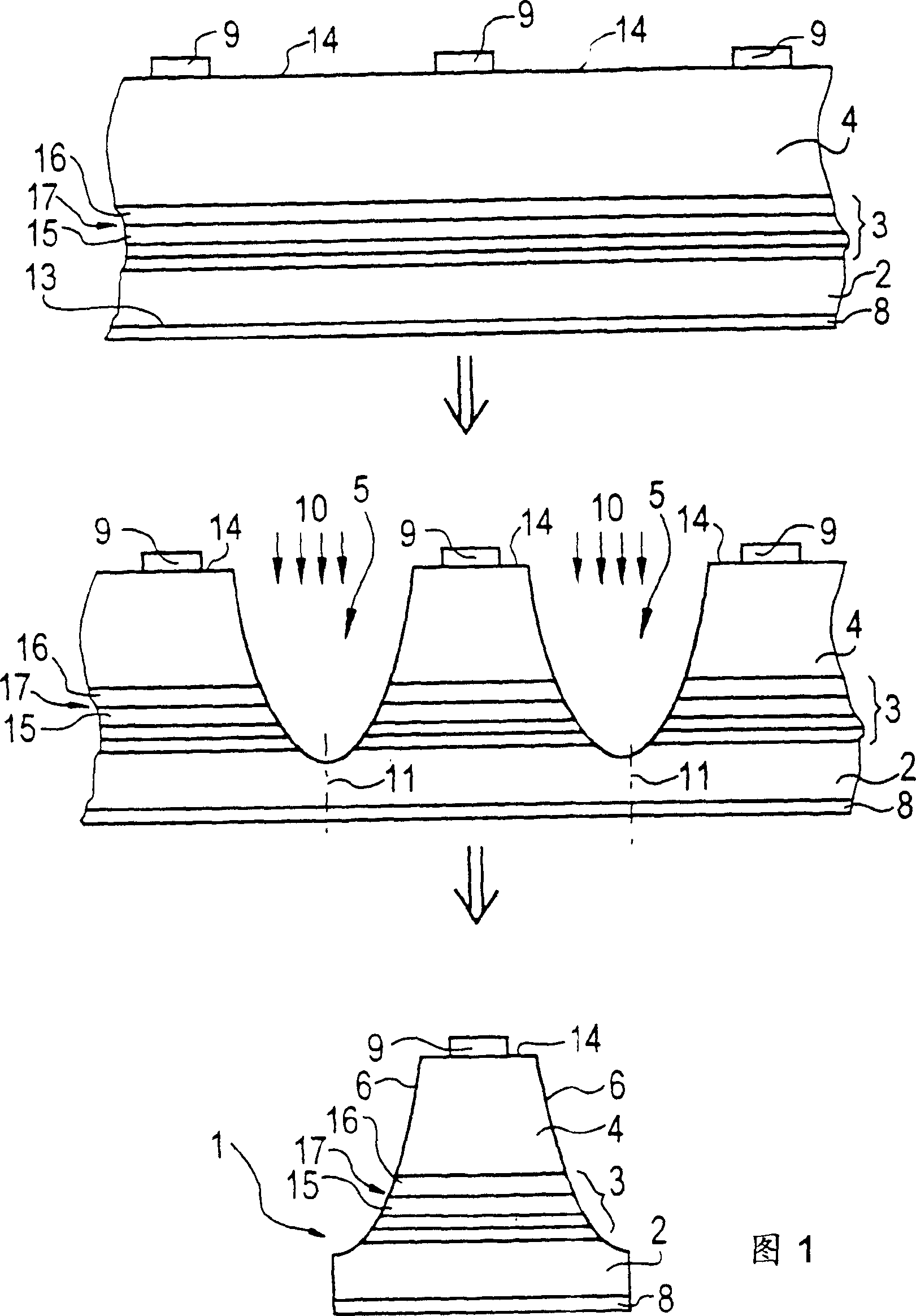
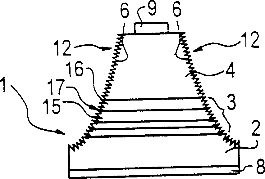
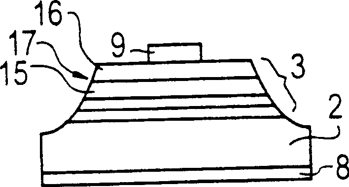
[0038] In these different figures the same components are each provided with the same associated reference numerals.

[0039] In the method according to FIG. 1, a layer sequence 3 is first deposited on a substrate disk 2 made of, for example, gallium arsenide, using metal-organic vapor phase epitaxy (MOVPE). This layer sequence is made of InGaAsP, for example, and has an active region 17 . The active region 17 is, for example, a Pn junction of a light emitting diode. The layer sequence 3 here has, for example, an n-type 15 and a p-type InGaAlP epitaxial layer 16 .

[0040] The active region 17 is constructed such that it emits light if a current is applied to it, and / or generates a voltage if the active region receives light. Such various active regions and the associated various fabrication methods are well known to those skilled in the art and will therefore not be described in detail here.

[0041] A window layer 4 , for example made of GaP or AlGaAs, is then deposited o...


PUM


Abstract

This invention concerns a process for producing at least one semiconductor body in which metal organic vapour phase epitaxy (MOVPE) is used to apply a layer sequence with an active zone to a substrate wafer. Dry etching is used on the layer sequence to form at least one mesa trench which is at least deep enough to cut through the active zone of the layer sequence. Subsequently, the composite of substrate wafer and layer sequence is cut through so that at least one semiconductor body with at least one mesa flank is produced.

Description

technical field [0001] The invention relates to a method for producing at least one semiconductor body on which a layer sequence with at least one active region is deposited on a substrate disk using metal-organic vapor phase epitaxy, and in this case The layer sequence on the semiconductor body is provided with at least one mesa trench. In particular, the invention relates to a method for using MOVPE ( M etal O rganic V apor P hase E A method for manufacturing a fluorescent diode chip with a mesa structure. Background technique [0002] A method for manufacturing MOVPE fluorescent diode chips is disclosed, for example, from the US patent document US-5,233,204. Here, a metal organic vapor phase epitaxy (MOVPE) technique is used to deposit an n-type first InGaAlP confinement layer, an n-type active InGaAlP layer and a p-type second InGaAlP confinement layer on a GaAs substrate disk fabricated heterostructures. A window layer made of AlGaAs, GaAsP or GaP is placed on t...

Claims


Application Information

Patent Timeline
Patent Type & Authority Patents(China)
IPC IPC(8): H01L21/302H01L21/301H01L21/306H01L21/3065H01L21/78H01L31/10H01L33/00H01L33/20H01L33/22
CPCH01L33/22H01L21/30621H01L33/20H01L33/0062H01L21/78H01L33/0095
Inventor O·肖恩菲尔德E·尼尔施尔
Owner SIEMENS AG
Why Eureka
Try Eureka