Semiconductor test structure and test method

A technology of test structure and test method, which is applied in semiconductor/solid-state device test/measurement, single semiconductor device test, semiconductor device, etc., can solve problems such as easy copper diffusion and difficult test, so as to improve stability and service life, The effect of reducing test error

Pending Publication Date: 2021-08-06
SHANGHAI HUALI MICROELECTRONICS CORP
View PDF7 Cites 2 Cited by
  • Summary
  • Abstract
  • Description
  • Claims
  • Application Information

AI Technical Summary

Problems solved by technology

However, since the nanoprobe needs to carry out surface treatment on the test sample during measurement, exposing the conductive layer whose main material is copper in the test structure, copper diffusion phenomenon is prone to occur in the measurement process (see Figure 5 ), which brings great difficulty to the test

Method used


Image

  • Semiconductor test structure and test method
  • Semiconductor test structure and test method
  • Semiconductor test structure and test method

Examples


Embodiment Construction

[0038] The specific implementation manner of the present invention will be described in more detail below with reference to schematic diagrams. The advantages and features of the present invention will be more apparent from the following description. It should be noted that all the drawings are in a very simplified form and use imprecise scales, and are only used to facilitate and clearly assist the purpose of illustrating the embodiments of the present invention.

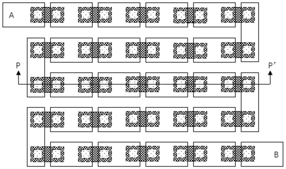
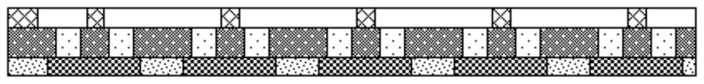
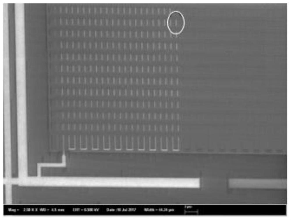
[0039] The invention provides a semiconductor testing structure and testing method. Figure 6 A top view of the semiconductor test structure provided in this embodiment, Figure 7 for Figure 6 The cross-sectional structure diagram of the semiconductor test structure described in along the QQ' direction. refer to Figure 6 and Figure 7 , the semiconductor test structure includes a first metal layer 100 and a second metal layer 300, wherein the first metal layer 100 includes a number of first metals 1 arranged...


PUM


Abstract

The invention provides a semiconductor test structure and a test method. The semiconductor test structure comprises a first metal layer, a second metal layer, and aplurality of electric contact pieces;the first metal layercomprises a plurality of first metals arranged at intervals; the second metal layer comprises a plurality of second metals which are arranged at intervals and arranged above the first metals in a staggered manner; the first metals and the second metals are connected end to end and electrically connected with each other through metal through holes to form a plurality of chain-shaped structures which are mutually connected in parallel and are connected end to end; and the plurality of electric contact pieces are correspondingly arranged above the second metal layer. According to the semiconductor test structure and the test method provided by the invention, the electric contact pieces are arranged above the second metal layer, so that the resistance of the semiconductor test structure is tested in a segmented manner, and the condition that the second metals are corroded due to contact with air or other reasons when the resistance is directly tested through the second metals is avoided, and therefore, the stability of the semiconductor test structure is improved, and the service life of the semiconductor test structure can be prolonged, and test errors are reduced.

Description

technical field [0001] The invention relates to the technical field of semiconductor testing, in particular to a semiconductor testing structure and testing method. Background technique [0002] There is a contact resistance (Contact Resistance, RC) at the connection between different layers in the IC circuit, and the contact resistance needs to have a low and stable resistance. If the resistance value of the contact resistance is too high, there will be a large voltage drop at the high resistance, thereby affecting the operation of the entire circuit. The contact resistance test is a common test item of the wafer reliability test (Wafer Acceptance Test, WAT). Since the resistance value of a single contact resistance is small, the direct measurement error is large, so in the WAT test, a single contact resistance is used as a unit to form a repeated chain structure (Chain) that is convenient for testing. refer to figure 1 and figure 2 , the common chain structure applies...

Claims


Application Information

Patent Timeline
Patent Type & Authority Applications(China)
IPC IPC(8): H01L23/544H01L21/66G01R27/02G01R31/26
CPCH01L22/34H01L22/32H01L22/14H01L22/20H01L23/544G01R31/2601G01R27/02
Inventor 武城段淑卿高金德
Owner SHANGHAI HUALI MICROELECTRONICS CORP
Why Eureka
Try Eureka