An rt detector suitable for lattice-mismatched epitaxial materials and its application

An epitaxial material, lattice mismatch technology, applied in the direction of instruments, heat measurement, measurement devices, etc., can solve the problems of lattice mismatch material large stress, large material deformation, long growth time, etc., to improve the effective receiving range. , The effect of avoiding large temperature deviation and reducing the probability of flying pieces

Active Publication Date: 2022-05-20
ZHONGSHAN DEHUA CHIP TECH CO LTD
View PDF14 Cites 0 Cited by
  • Summary
  • Abstract
  • Description
  • Claims
  • Application Information

AI Technical Summary

Problems solved by technology

For heteroepitaxy materials with a large degree of mismatch with the crystal lattice, in order to ensure the complete relaxation of the lattice of the mismatched material and avoid the increase of lattice dislocations, the composition change rate of the composition gradient buffer layer should not be too fast, so the buffer The thickness of the layers is relatively thick, and the growth time is long. More importantly, because the stress between the lattice mismatched materials is large and it is difficult to be fully released, the overall material deformation is relatively large during the preparation process, causing the reflection signal to deviate from the effective reception. The area is far away, the traditional RT and TC temperature control methods are no longer applicable, and the sudden increase in the calculation amount using the difference comparison method leads to a delay effect. Therefore, the monitoring during the growth of the epitaxial wafer is correspondingly more difficult

Method used


Image

  • An rt detector suitable for lattice-mismatched epitaxial materials and its application
  • An rt detector suitable for lattice-mismatched epitaxial materials and its application
  • An rt detector suitable for lattice-mismatched epitaxial materials and its application

Examples


Embodiment Construction

[0044] In order to describe the technical content, achieved goals and effects of the present invention in detail, the following descriptions will be made in conjunction with the embodiments and accompanying drawings. The test methods used in the examples are conventional methods unless otherwise specified; the used materials, reagents, etc., are commercially available reagents and materials unless otherwise specified.

[0045] In the description of the present invention, it should be understood that the orientation descriptions, such as up, down, front, back, left, right, etc. indicated orientations or positional relationships are based on the orientations or positional relationships shown in the drawings, and are only In order to facilitate the description of the present invention and simplify the description, it does not indicate or imply that the device or element referred to must have a specific orientation, be constructed and operated in a specific orientation, and thus sh...


PUM

PropertyMeasurementUnit
wavelengthaaaaaaaaaa
conversion efficiencyaaaaaaaaaa

Abstract

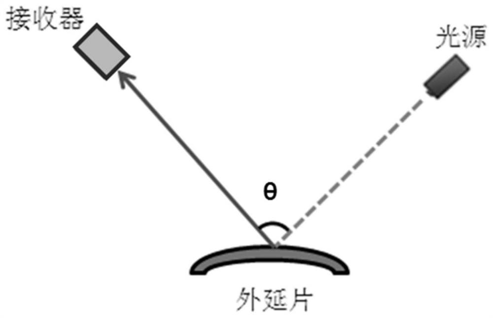
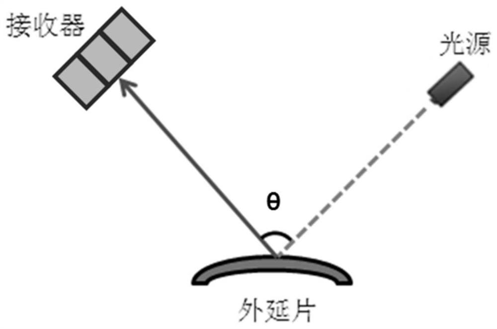
The invention discloses an RT detector suitable for lattice-mismatched epitaxial materials and its application. The RT detector suitable for lattice-mismatched epitaxial materials includes a light source and several sub-receivers; the several sub-receivers The distribution method is an array distribution; the light source is used to emit incident light, and the incident light propagates to the surface of the peripheral epitaxial wafer to form an optical signal; the sub-receiver is used to receive the optical signal formed by the corresponding epitaxial wafer, and The received optical signal is photoelectrically converted to obtain an electrical signal; it realizes the precise monitoring of the growth temperature during the growth process of the lattice mismatch structure epitaxial wafer.

Description

technical field [0001] The invention relates to the field of growth and preparation of semiconductor materials, in particular to an RT detector suitable for lattice-mismatched epitaxial materials and an application thereof. Background technique [0002] The growth and preparation of epitaxial materials by MOCVD requires precise monitoring of the growth temperature. There are two commonly used monitoring methods, namely (RT) and (TC). Among them, RT is the temperature of the wafer surface, which is realized by monitoring the reflectance curve, and TC is the temperature of the graphite disk, which is detected by a thermocouple. For lattice-mismatched multi-junction cells, during the growth process, in addition to the stress caused by the difference in thermal expansion coefficient between the epitaxial layer material and the substrate under high temperature conditions, the stress introduced by the growth of the lattice-mismatched material will cause the epitaxial wafer to ben...

Claims


Application Information

Patent Timeline
Patent Type & Authority Patents(China)
IPC IPC(8): G01K11/00G01N21/55H01L31/12
CPCG01K11/00G01N21/55H01L31/125Y02P70/50
Inventor 刘雪珍张小宾高熙隆刘建庆杨文奕
Owner ZHONGSHAN DEHUA CHIP TECH CO LTD
Why Eureka
Try Eureka