Silicon on insulator (SOI)-based GaN wafer and preparation method thereof

A wafer and growth method technology, applied in the field of SOI-based GaN wafers and their preparation, can solve the problems of inability to prepare low-defect density, large-size GaN wafers, etc., and achieve the effect of avoiding excessive warping

Pending Publication Date: 2021-08-13
SHANGHAI INST OF MICROSYSTEM & INFORMATION TECH CHINESE ACAD OF SCI
View PDF4 Cites 0 Cited by
  • Summary
  • Abstract
  • Description
  • Claims
  • Application Information

AI Technical Summary

Problems solved by technology

[0005] The technical problem to be solved by the present invention is to provide an SOI-based GaN wafer and its preparation method, which overcomes the defects that the existing technology cannot prepare GaN wafers with low defect density, large size, and no device crosstalk

Method used


Image

  • Silicon on insulator (SOI)-based GaN wafer and preparation method thereof
  • Silicon on insulator (SOI)-based GaN wafer and preparation method thereof
  • Silicon on insulator (SOI)-based GaN wafer and preparation method thereof

Examples


Embodiment 1

[0035] 1. Select the SOI substrate material with the following parameters, as shown in Table 1 below:

[0036] Table 1

[0037]

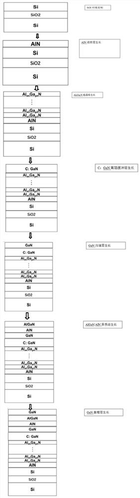
[0038] 2. Deposit sequentially on the SOI surface from bottom to top by MOCVD method, as shown in Table 2 below:

[0039] Table 2

[0040]

[0041] The specific preparation method of the GaN wafer: firstly, in the MOCVD chamber, the surface of the SOI wafer is pretreated with TMAl for 12-15s, the temperature is 1060°C, and the carrier gas is H 2 , the pressure is 100mbar, and then the material preparation method for growing each layer in turn is shown in Table 3 below:

[0042] table 3

[0043]

[0044] The specific measured performance parameters are shown in Table 4:

[0045] Table 4

[0046]

[0047] AlGaN barrier layer thickness 23.55nm (center) and 23.58nm (edge).

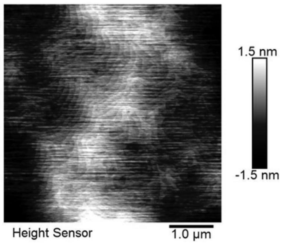
[0048] like figure 1 As shown, the structure shows that the roughness RMS is only 0.6nm;

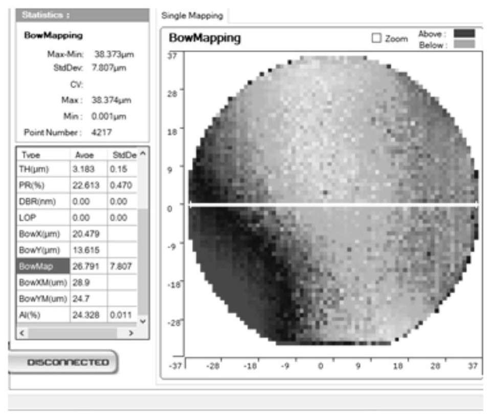
[0049] like figure 2 As shown, the results show that the warpage is...


PUM

PropertyMeasurementUnit
thicknessaaaaaaaaaa
thicknessaaaaaaaaaa
thicknessaaaaaaaaaa

Abstract

The invention relates to an SOI-based GaN wafer and a preparation method thereof. The GaN wafer sequentially comprises an SOI substrate, an AlN nucleating layer, an AlxGayN superlattice, a carbon-doped gallium nitride C: GaN buffer layer, a GaN channel layer, an AlGaN/AlN heterojunction and a GaN cap layer from bottom to top. Optimized SOI customized parameters and a C: GaN/AlGaN/AlN heterojunction technology are adopted, and lattice mismatch of heterojunction is utilized to match thermal mismatch between GaN and SOI, so that the problem that an SOI-based GaN wafer is excessively warped and even cracked in the high-temperature growing and cooling processes is avoided, and single-chip integration for GaN power electronics is facilitated.

Description

technical field [0001] The invention belongs to the field of GaN wafer and its preparation, in particular to a GaN wafer for SOI base and its preparation method. Background technique [0002] Single-chip integrated gallium nitride (GaN) power electronics can effectively suppress the parasitic effects introduced by packaging, PCB connection and driving circuits, etc., and can greatly reduce chip size and quantity, and improve design flexibility. [0003] GaN on silicon (GaN-on-Si) has the advantages of low cost and large size, and is the development trend of GaN wafers. However, device crosstalk and background effects caused by sharing silicon substrates make GaN-on-Si single-chip Integration is extremely challenging. If silicon-on-insulator (SOI)-based GaN (GaN-on-SOI) is used, with the help of SOI BOX layer (SiO 2 ) full dielectric isolation characteristics, which can effectively eliminate crosstalk, suppress background effects, and reduce on-resistance degradation. [0...

Claims


Application Information

Patent Timeline
Patent Type & Authority Applications(China)
IPC IPC(8): H01L29/778H01L27/12H01L21/335
CPCH01L29/7787H01L27/1203H01L29/66462
Inventor 郑理程新红俞跃辉
Owner SHANGHAI INST OF MICROSYSTEM & INFORMATION TECH CHINESE ACAD OF SCI
Why Eureka
Try Eureka