


Quick Research
Generate reliable direction feasibility study reports for your R&D in just a few steps.

Technical Q&A
Discover and master advanced knowledge NOW. Basics, ideas, possibilities, all at once.

Find Solutions
As an expert in R&D theories, this can generate solutions to your technical problems instantly.

Evaluate Feasibility
Analyze your overall solution with one click, know your potential R&D risks in advance.

Monitor Landscape
Get weekly tech updates, stay abreast of the latest tech innovations and key insights.
Semiconductor packages
A technology of semiconductors and semiconductor tubes, applied in the field of semiconductor packaging, which can solve the problems of expensive alignment and robotic equipment, insufficient performance of wire bonding technology, and inconvenience to end users
- Summary
- Abstract
- Description
- Claims
- Application Information
AI Technical Summary
Problems solved by technology
Method used
Image

Examples
Embodiment Construction
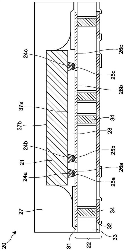
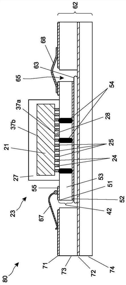
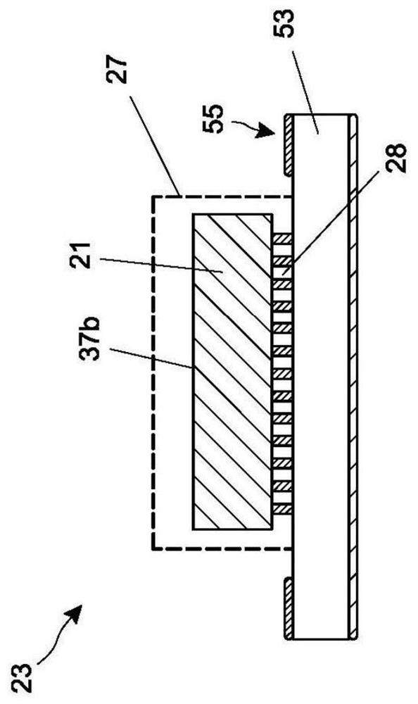
[0031] Various embodiments disclosed herein relate to semiconductor packaging. For example, embodiments disclosed herein may be particularly beneficial for packaging radio frequency (RF) dies or chips. However, it should be understood that the embodiments disclosed herein are also beneficial for any other type of semiconductor die.
[0032] A semiconductor die or chip includes an active side that may have active semiconductor components, such as transistors, fabricated therein. The active side may also include bond pads, which may serve as an interface between the semiconductor die and external circuits and components. For example, bond pads may include input and / or output pads for transmitting and / or receiving signals, power pads for receiving a supply voltage, and / or ground pads for grounding. Although various examples of bond pads have been described, a semiconductor die may include bond pads that serve multiple functions. After fabrication, the semiconductor die may be ...
PUM
 Abstract
Description
Claims
Application Information
 - R&D Engineer
- R&D Manager
- IP Professional
- Industry Leading Data Capabilities
- Powerful AI technology
- Patent DNA Extraction
Browse by: Latest US Patents, China's latest patents, Technical Efficacy Thesaurus, Application Domain, Technology Topic, Popular Technical Reports.
© 2024 PatSnap. All rights reserved.Legal|Privacy policy|Modern Slavery Act Transparency Statement|Sitemap|About US| Contact US: help@patsnap.com