
A driving circuit for radio frequency transceiver

A drive circuit, radio frequency transceiver technology, applied in the direction of electrical components, transmission systems, etc., can solve the problems of inaccurate delay, no overlap risk of overlapping circuits, etc., and achieve the effect of small size and low cost

Active Publication Date: 2021-09-24
成都华兴大地科技有限公司
View PDF10 Cites 0 Cited by
  • Summary
  • Abstract
  • Description
  • Claims
  • Application Information

AI Technical Summary

Problems solved by technology

[0004] The non-overlapping circuits in the prior art are mainly produced by the principle of inverters and time delays. In the CMOS process, due to the manufacturing deviation of active and passive devices, the time delay will be inaccurate, resulting in non-overlapping. There is a risk of overlapping circuits

Method used


Image

  • A driving circuit for radio frequency transceiver
  • A driving circuit for radio frequency transceiver

Examples


Embodiment Construction

[0016] The present invention will be described in detail below in conjunction with the accompanying drawings.

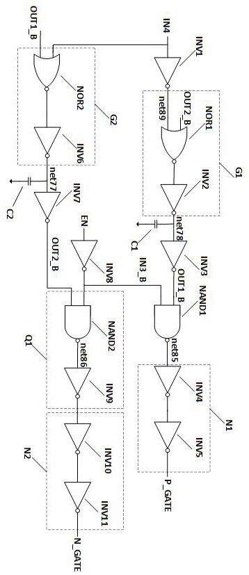
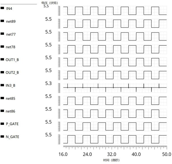
[0017] Such as figure 1 As shown, the circuit of the present invention includes 11 inverters INV1, INV2, INV3, INV4, INV5, INV6, INV7, INV8, INV9, INV10, INV11, 2 NAND gates NAND1, NAND2, 2 NOR gates NOR1 , NOR2 and two capacitors C1, C2, wherein the first NOR gate NOR1 and the second inverter INV2 form the first OR gate G1, and the second NOR gate NOR2 and the sixth inverter INV6 form the second OR gate G2, the fourth inverter INV4 and the fifth inverter INV5 constitute the first output buffer unit N1, the tenth inverter INV10 and the eleventh inverter INV11 constitute the second output buffer unit N2, the second NAND gate NAND2 and the ninth inverter INV9 form the first AND gate Q1:

[0018] The input terminal of the first inverter INV1 and one input terminal of the second OR gate G2 are both connected to the input pulse signal IN4. The first inverter INV1 is us...


PUM


Abstract

The invention belongs to the technical field of integrated circuits, and in particular relates to a driving circuit for radio frequency transceiver. The present invention uses the reference pulse input signal to first turn off the originally turned-on power transistor, and then generates a turn-off signal together with the reference pulse input signal to turn on the originally turned-off power transistor, thereby realizing a precise non-overlapping power supply process. No matter how the CMOS manufacturing process changes, the non-overlapping process of power supply will not be affected, the compound semiconductor MMIC chip is well protected, and the size is small and the cost is low.

Description

technical field [0001] The invention belongs to the technical field of integrated circuits, and in particular relates to a driving circuit for radio frequency transceiver. Background technique [0002] The RF transceiver front-end in radar system applications mainly adopts the principle of time division multiplexing, and most of them use compound semiconductors to manufacture MMIC chips to improve system performance. Therefore, the transmitting and receiving power supplies use pulsed switching power supplies, and the transmitting and receiving power supplies cannot overlap. [0003] The non-overlapping circuit can be realized by the front-end control signal, and then control the power transistor to realize non-overlapping power supply. [0004] The non-overlapping circuit in the prior art is mainly produced by using the principle of inverter and time delay. In the CMOS process, due to the manufacturing deviation of active and passive devices, the time delay will be inaccurat...

Claims


Application Information

Patent Timeline
Patent Type & Authority Patents(China)
IPC IPC(8): H04B1/40
CPCH04B1/40
Inventor 李俊美龙飞王洪全
Owner 成都华兴大地科技有限公司
Learn More