Processing system and method for material parts

A processing system and material technology, which is applied in the manufacture of electrical components, conveyor objects, semiconductor/solid-state devices, etc., can solve the problems of long process cycle and surface damage of wafers, and reduce the difficulty of installation and shoveling. cost reduction effect

Pending Publication Date: 2021-08-24
苏州辰轩光电科技有限公司
View PDF0 Cites 0 Cited by
  • Summary
  • Abstract
  • Description
  • Claims
  • Application Information

AI Technical Summary

Problems solved by technology

[0004] In addition, due to the high precision requirements on the surface of the wafer, it is bound to require that the wear of the surface of the wafer in the above process and the subsequent collection process should be as small as possible. Transfer, which results in a long process cycle, and the inevitable contact action and adsorption force will more or less cause damage to the surface of the wafer

Method used


Image

  • Processing system and method for material parts
  • Processing system and method for material parts
  • Processing system and method for material parts

Examples


Embodiment Construction

[0036] The following will clearly and completely describe the technical solutions in the embodiments of the present invention with reference to the accompanying drawings in the embodiments of the present invention. Obviously, the described embodiments are only some, not all, embodiments of the present invention. Based on the embodiments of the present invention, all other embodiments obtained by persons of ordinary skill in the art without making creative efforts belong to the protection scope of the present invention.

[0037] It should be noted that in the description of the present invention, terms such as "first" and "second" are only used to describe the purpose and distinguish similar objects, there is no sequence between the two, and they cannot be interpreted as indicating or imply relative importance. In addition, in the description of the present invention, unless otherwise specified, "plurality" means two or more.

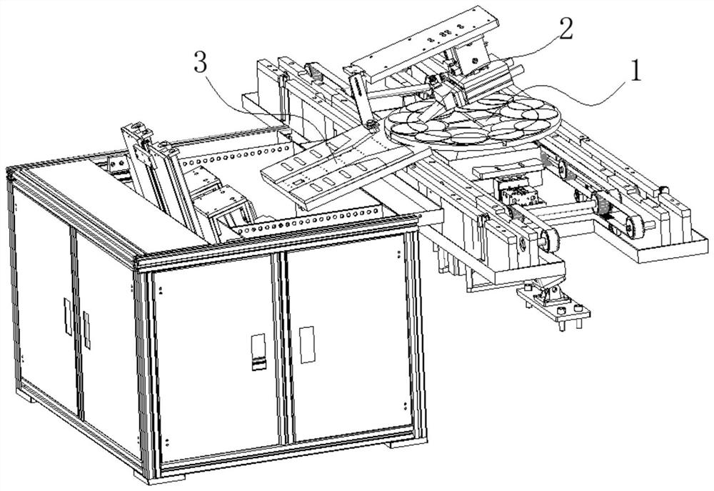
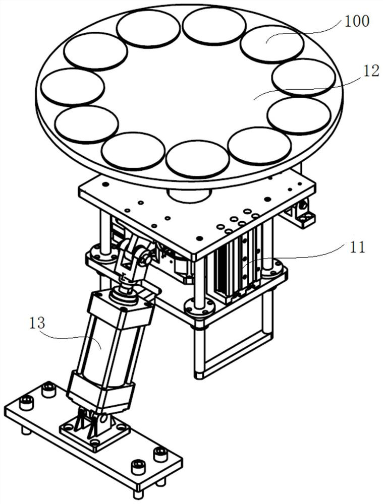
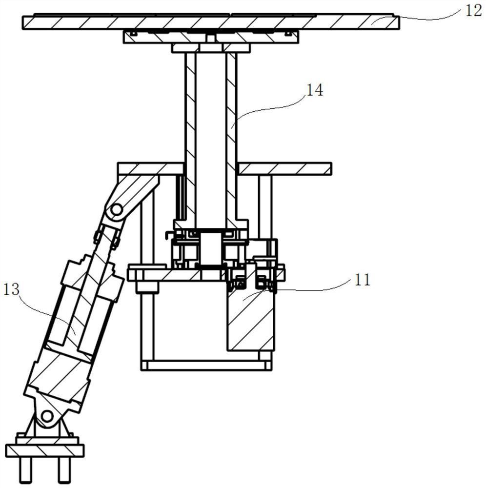
[0038] combine Figure 1 to Figure 5 As shown, t...


PUM


Abstract

The invention discloses a processing system for material parts, and the system comprises a wax pasting mechanism, a transferring mechanism and a separating mechanism which are used for the materials, and the separating mechanism comprises a bearing unit, a shovel piece unit, a driving unit and a guiding unit. The bearing unit can rotate from a horizontal plane to an inclined plane under the action of the driving unit and then is arranged corresponding to the shovel sheet unit; a material part which is bonded through a wax body is borne on the bearing unit; the shovel piece unit can push the material piece to move relative to the supporting platform in a staggered mode so that the material piece can be separated from the supporting platform. The guiding unit comprises a guiding groove, the guiding groove is filled with flowing drainage liquid, and the drainage liquid can bear and drain the material piece to move from the inlet end to the outlet end. The wafer guiding and collecting device at least has the following advantages that the wafer does not make contact with an external mechanism in the guiding and collecting process while the shoveling difficulty is effectively reduced, and the phenomenon that the surface of the wafer is damaged is avoided.

Description

technical field [0001] The invention relates to the technical field of automation equipment, in particular to a processing system and method for materials. Background technique [0002] The statements in this section only provide background information related to the present disclosure and may not constitute prior art. [0003] Wafer is the carrier used in the production of integrated circuits, mostly referring to single crystal silicon wafers. Single crystal silicon wafers are drawn and refined from ordinary silica sand, and are made into single crystal silicon rods through a series of measures of dissolution, purification and distillation. After the single crystal silicon rods are polished and sliced, they become wafers. In the current production process, the surface of the wafer needs to be processed, and the wax dripping process is relatively common, so that the wafer will be bonded to the support after the liquid wax solidifies. Since the thickness of the wafer is rel...

Claims


Application Information

Patent Timeline
Patent Type & Authority Applications(China)
IPC IPC(8): H01L21/67H01L21/677H01L21/687
CPCH01L21/67092H01L21/6715H01L21/67703H01L21/68714
Inventor 胡小辉
Owner 苏州辰轩光电科技有限公司
Why Eureka
Try Eureka