Metrology of semiconductor devices in electron micrographs using fast marching level sets

A level set, fast technology, applied in the field of image processing and measurement based on deep learning, can solve problems such as poor signal-to-noise ratio, poor contrast, and difficult image processing

Pending Publication Date: 2021-08-27
FEI CO
View PDF0 Cites 0 Cited by
  • Summary
  • Abstract
  • Description
  • Claims
  • Application Information

AI Technical Summary

Problems solved by technology

[0002] Processing of images obtained by electron microscopy is difficult due to typical image quality (possibly with poor contrast and poor signal-to-noise ratio)
For example, such poor image quality can make it difficult to use the image for structural analysis (e.g. the measurement of structures in the image) due to the lack of definition of structure boundaries
While various image processing techniques can be used to overcome some of the difficulties, these techniques often require manual control by highly skilled technicians

Method used


Image

  • Metrology of semiconductor devices in electron micrographs using fast marching level sets
  • Metrology of semiconductor devices in electron micrographs using fast marching level sets
  • Metrology of semiconductor devices in electron micrographs using fast marching level sets

Examples


Embodiment Construction

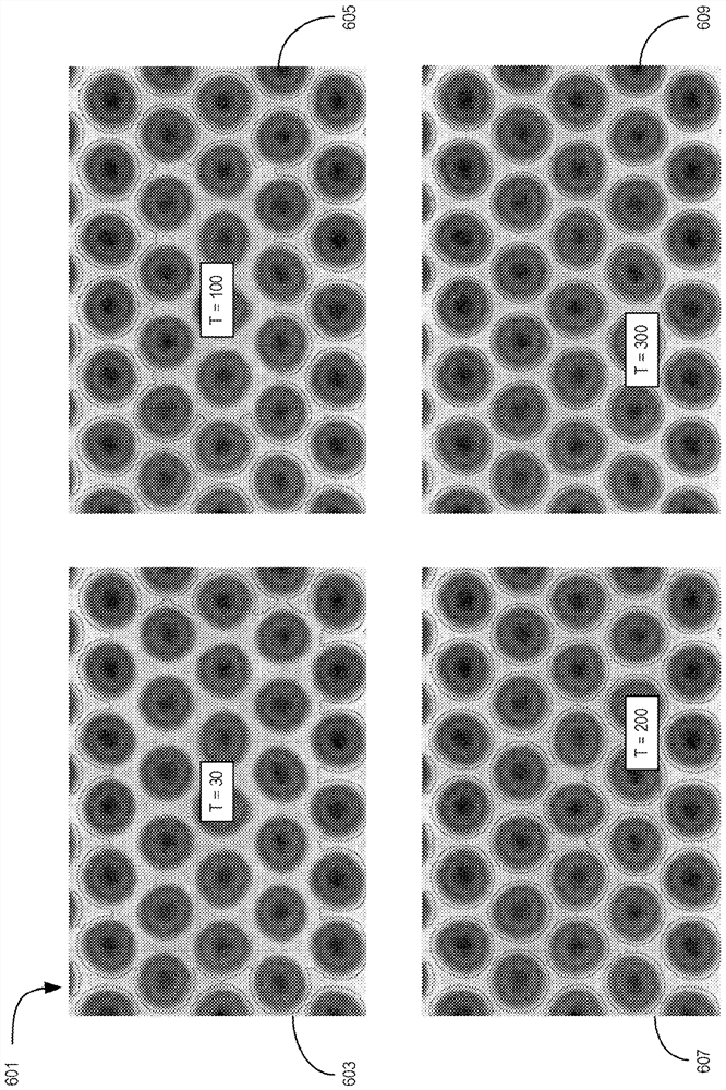
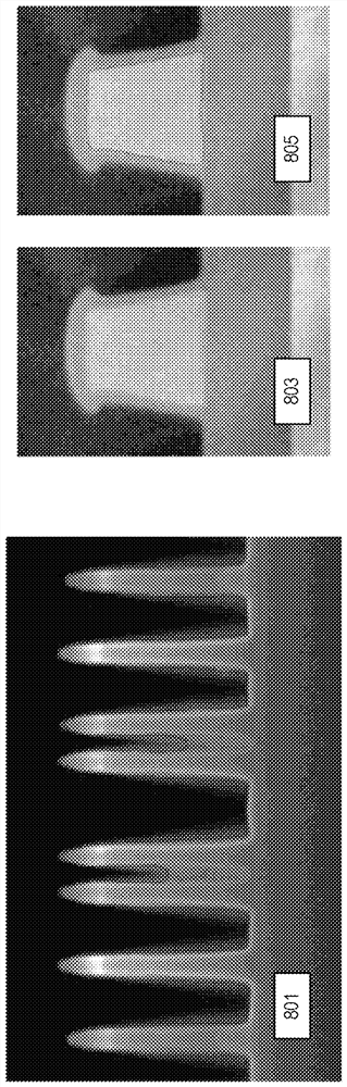
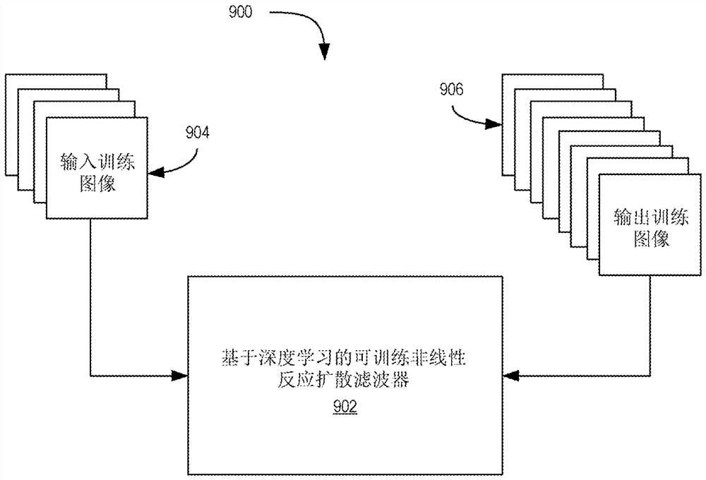
[0017] Embodiments of the invention are described below in the context of an electron microscope performing segmentation and metrology techniques using a mixture of conventional and deep learning based algorithms and models. For example, an electronic image can be smoothed and filtered using a trained model that then has one or more fast-marching level set algorithms implemented on it to find one or more boundaries within the image. The delineated boundaries are then used to anchor the metric algorithm to measure various aspects of the ROI in the image. The various embodiments disclosed herein provide examples of implementing the disclosed technology and should not be taken as limitations of the disclosed technology.

[0018] As used in this application and the claims, the singular forms "a", "an" and "the" include plural referents unless the context clearly dictates otherwise. In addition, the term "comprising" means "comprising". Furthermore, the term "coupled" does not ex...


PUM


Abstract

The invention relates to metrology of semiconductor devices in electron micrographs using fast marching level sets. Apparatuses and methods for metrology on devices using fast marching level sets are disclosed herein. An example method at least includes initiating a fast marching level set seed on an image, propagating a fast marching level set curve from the fast marching level set seed to locate boundaries of a plurality of regions of interest within the image, and performing metrology on the regions of interest based in part on the boundaries.

Description

technical field [0001] The present invention relates generally to image processing and automated metrology, and more particularly to deep learning-based image processing and metrology of charged particle-based micrographs using fast-marching level sets. Background technique [0002] Processing of images obtained by electron microscopy is difficult due to typical image quality (possibly with poor contrast and poor signal-to-noise ratio). For example, such poor image quality can make it difficult to use the image for structural analysis (e.g., the measurement of structures in the image) due to the lack of definition of structure boundaries. While various image processing techniques can be used to overcome some of the difficulties, these techniques usually require manual control by a highly skilled technician. In most use cases, automated and efficient analysis is desired. Contents of the invention [0003] Apparatus and methods for metrology of devices using fast-traveling...

Claims


Application Information

Patent Timeline
Patent Type & Authority Applications(China)
IPC IPC(8): G06K9/00G06K9/32G06N3/04G06N3/08
CPCG06N3/04G06N3/08G06V20/693G06V20/695G06V20/698G06V10/25G06T2207/10056G06T2207/20081G06T2207/20084G06T2207/30148G06T7/12G06T7/149G06N20/10G06N20/20G06N5/01G06N7/01G06T7/136G06T7/11G06T5/002G06N20/00G06T2207/10061G06V10/30G03F7/70666G03F7/70091G06T7/0004
Inventor U·阿迪加
Owner FEI CO
Why Eureka
Try Eureka