Check patentability & draft patents in minutes with Patsnap Eureka AI!

Phase change memory and preparation method thereof

A phase-change memory and contact hole technology, which is applied in semiconductor/solid-state device manufacturing, semiconductor devices, electric solid-state devices, etc., can solve the problems of low-quality film layers of phase-change memory, improve layout flexibility, improve film layer quality, effect of device size

Active Publication Date: 2021-08-27
YANGTZE ADVANCED MEMORY INDUSTRIAL INNOVATION CENTER CO LTD
View PDF7 Cites 0 Cited by
  • Summary
  • Abstract
  • Description
  • Claims
  • Application Information

AI Technical Summary

Problems solved by technology

[0003] The purpose of the present invention is to provide a phase change memory to solve the problem of low film quality of the existing phase change memory

Method used


Image

  • Phase change memory and preparation method thereof
  • Phase change memory and preparation method thereof
  • Phase change memory and preparation method thereof

Examples


preparation example Construction

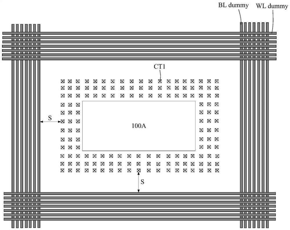
[0079] For the phase change memory as mentioned above, the following combination Figure 4a The preparation method thereof will be described. Such as Figure 4a As shown, the preparation method of the phase change memory may specifically include: respectively forming an auxiliary bit line layer and an auxiliary word line layer in two planes parallel to each other, for example, the auxiliary bit line layer may be formed in the first plane, and the second forming an auxiliary word line layer in a second plane parallel to the plane; and etching the auxiliary word line layer and the auxiliary bit line layer to form a first contact hole; covering the sidewall of the first contact hole with isolation layer, and fill the first contact hole with a conductive material layer to form a first contact plug.

[0080] Based on the above preparation method, the first contact plug that is electrically insulated from the auxiliary bit line layer and the auxiliary word line layer can be formed...


PUM


Abstract

The invention provides a phase change memory and a preparation method thereof. The phase change memory comprises a first contact plug which sequentially penetrates through an auxiliary word line layer and an auxiliary bit line layer, and an isolation layer is arranged on the outer side wall of the first contact plug, so that mutual interference between a conductive material layer in the first contact plug and an auxiliary word line / auxiliary bit line can be avoided. Thus, the auxiliary bit lines, the auxiliary word lines and the first contact plugs can be flexibly arranged, the situation that areas with too low pattern density exist in the corresponding bit line layers and the word line layers is prevented, the film layer quality of the prepared bit line layers and the prepared word line layers can be improved, and the number of the first contact plugs can be increased. In addition, due to the fact that the arrangement areas of the auxiliary bit lines, the auxiliary word lines and the first contact plugs can allow space overlapping, the size of the device can be effectively reduced.

Description

technical field [0001] The invention relates to the technical field of semiconductors, in particular to a phase-change memory and a preparation method thereof. Background technique [0002] The rapid development of information technology requires a large number of high-performance storage devices. Low voltage, low power consumption, high speed and high density are the inevitable development trends of storage technology. Phase change memory PCM is a new generation of non-volatile solid-state semiconductor memory developed on the basis of CMOS integrated circuits, which has many advantages compared with today's mainstream products. For example, in terms of storage density, the current mainstream memory has a limit on the technology node of more than 20 nanometers, and cannot be further compactly integrated; while the phase change memory can reach the order of 5 nanometers. And, in terms of storage speed, the phase change resistance of phase change memory is 100 times faster t...

Claims


Application Information

Patent Timeline
IPC IPC(8): H01L23/528H01L21/768H01L27/24
CPCH01L23/528H01L21/76831H01L2221/1057H10B63/80
Inventor 张曙王晓娟雷威锋刘峻张恒
Owner YANGTZE ADVANCED MEMORY INDUSTRIAL INNOVATION CENTER CO LTD
Features
  • R&D
  • Intellectual Property
  • Life Sciences
  • Materials
  • Tech Scout
  • Unparalleled Data Quality
  • Higher Quality Content
  • 60% Fewer Hallucinations
Learn More