Semiconductor material stress measurement system and method based on photoelastic modulation technology

A material stress and measurement system technology, which is applied in the direction of material analysis, measurement device, and material analysis by optical means, can solve problems such as the inability to meet the measurement needs, achieve the requirements of overcoming the stress of the measured sample, improve sensitivity and The effect of stability and improving test efficiency

Pending Publication Date: 2021-09-03
彭海鲸
View PDF1 Cites 2 Cited by
  • Summary
  • Abstract
  • Description
  • Claims
  • Application Information

AI Technical Summary

Problems solved by technology

And adopt photoelastic modulation device and lock-in amplifier technology to measure birefringence in the prior art and also be limited by some conditions, such as some techniques need to rotate the measured sample to obtain the size and direction of birefringence; It is not necessary to rotate the measured sample to obtain the size and direction of the birefringence, but it is required that the phase generated by the birefringence of the measured sample must be small enough to approximate the angle, so it cannot meet the needs of actual measurement

Method used


Image

  • Semiconductor material stress measurement system and method based on photoelastic modulation technology
  • Semiconductor material stress measurement system and method based on photoelastic modulation technology
  • Semiconductor material stress measurement system and method based on photoelastic modulation technology

Examples


Embodiment Construction

[0033] The following will clearly and completely describe the technical solutions in the embodiments of the present invention with reference to the accompanying drawings in the embodiments of the present invention. Obviously, the described embodiments are only some, not all, embodiments of the present invention. Based on the embodiments of the present invention, all other embodiments obtained by persons of ordinary skill in the art without creative efforts fall within the protection scope of the present invention.

[0034] It should be noted that, in the case of no conflict, the embodiments of the present invention and the features in the embodiments can be combined with each other.

[0035] The present invention will be further described below in conjunction with the accompanying drawings and specific embodiments, but not as a limitation of the present invention.

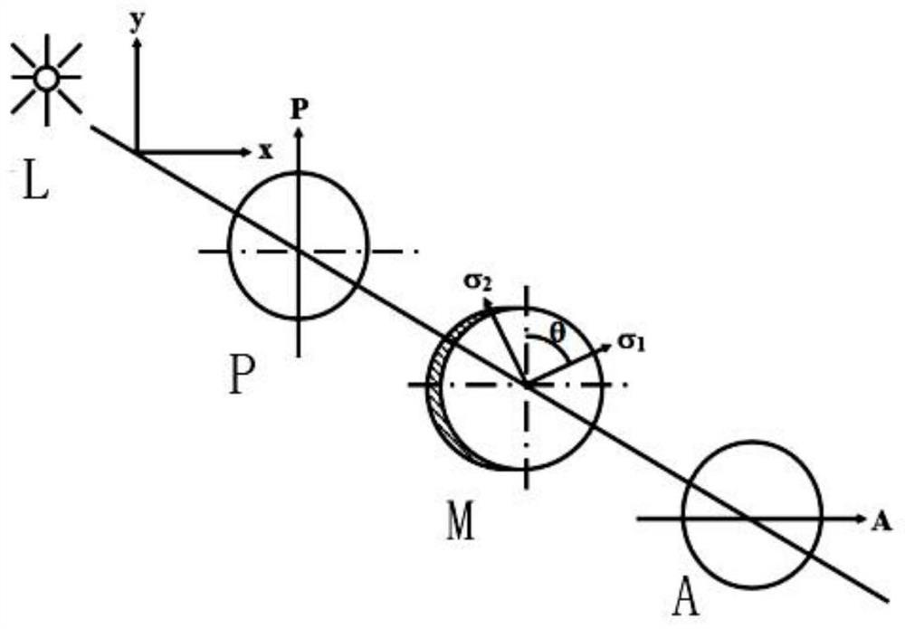
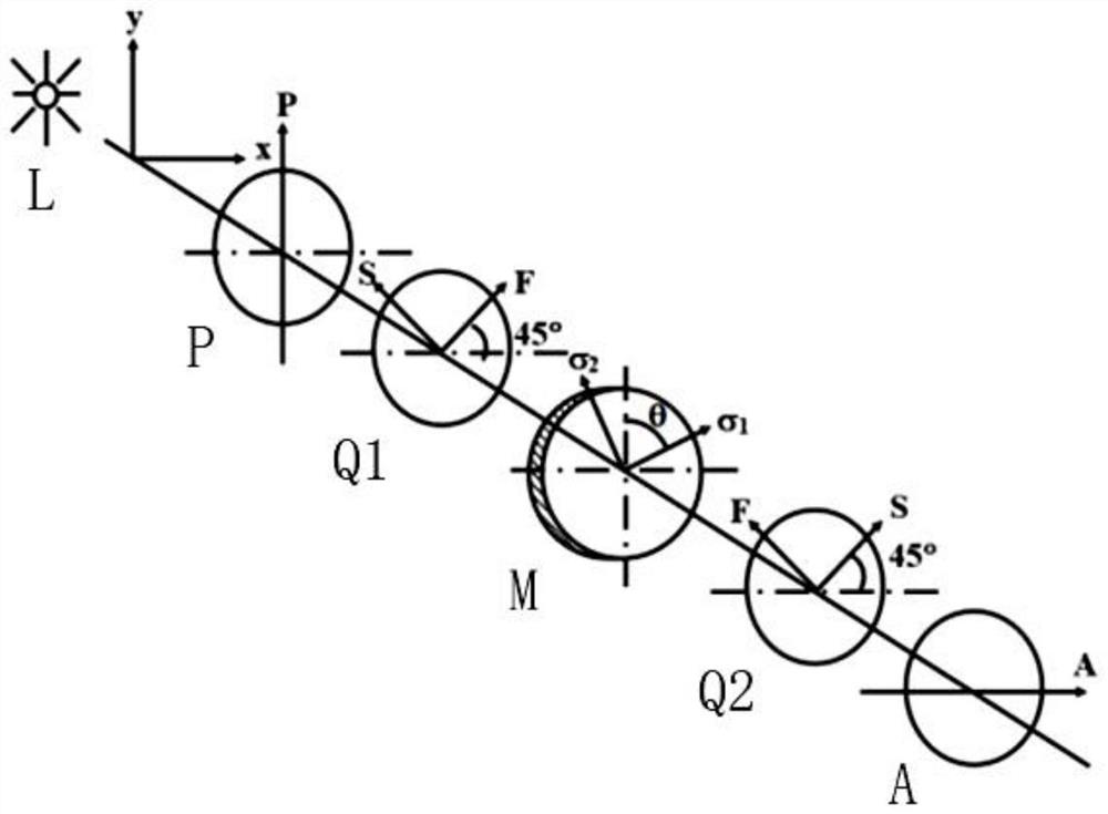
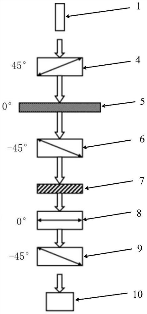
[0036] The present invention includes a semiconductor material stress measurement system based on photoelastic m...


PUM

PropertyMeasurementUnit
wavelengthaaaaaaaaaa

Abstract

The invention relates to the technical field of electronic equipment control, in particular to a semiconductor material stress measurement system based on a photoelastic modulation technology. The system comprises a laser light source, at least one reflector, a through hole, a polarizer, a photoelastic modulator, a first wave plate, a measured sample, a second wave plate, an analyzer and an infrared detector which are arranged in sequence, a laser beam emitted by the laser light source is guided into a measuring light path through at least one reflector, the polarizer converts the laser beam into linearly polarized light, the laser beam passes through the photoelastic modulator and then is converted into modulated polarized light which is continuously switched back and forth from the linearly polarized light to circularly polarized light, the modulated polarized light passes through a measured sample to form a birefringence signal, the infrared detector converts the birefringence signal into an electric signal, and the electric signal is transmitted to a computer for processing through the measuring circuit. The system has the beneficial effects that the requirement of other methods based on photoelastic modulation on the stress of the tested sample is met, and the tested sample in the system does not need to rotate.

Description

technical field [0001] The invention relates to the technical field of electronic equipment control, in particular to a semiconductor material stress measurement system and method based on photoelastic modulation technology. Background technique [0002] The traditional method of using birefringence technology to measure the stress of semiconductor materials is generally based on infrared photoelastic technology, using a plane or circular polarized light system to measure the birefringence of the material to measure the stress state in the material, where figure 1 Shown is a plane polarized light measurement system, including a light source L, a polarizer P, a sample M to be tested, and an analyzer A; figure 2 Shown is a circularly polarized light measurement system, including a light source L, a polarizer P, a quarter-wave plate Q1, a sample M to be measured, a quarter-wave plate Q2, and an analyzer A. The advantage of using a planar or circularly polarized light system t...

Claims


Application Information

Patent Timeline
Patent Type & Authority Applications(China)
IPC IPC(8): G01N21/01G01N21/23
CPCG01N21/01G01N21/23
Inventor 彭海鲸
Owner 彭海鲸
Why Eureka
Try Eureka