Chip metal wire, manufacturing method thereof and wafer

A manufacturing method and metal wire technology, which are applied in semiconductor/solid-state device components, semiconductor/solid-state device testing/measurement, semiconductor devices, etc., can solve problems such as saw blade cutting skew, chip function failure, and affecting cutting quality

Pending Publication Date: 2021-09-07
BEIJING SMARTCHIP MICROELECTRONICS TECH COMPANY +3
View PDF0 Cites 0 Cited by
  • Summary
  • Abstract
  • Description
  • Claims
  • Application Information

AI Technical Summary

Problems solved by technology

When using a saw blade to cut a wafer, because the fuse exists in the scribe line, the material composition in the scribe line is uneven (the fuse is copper wire, and the scribe is SiO2), and the pressure on both sides of the saw blade in the scribe line is inconsistent, resulting in cutting by the saw blade Skew, on the one hand, affects the cutting quality, on the other hand, it causes some fuses to fail to cut and break, and the chip function will fail in subsequent chip applications

Method used


Image

  • Chip metal wire, manufacturing method thereof and wafer
  • Chip metal wire, manufacturing method thereof and wafer
  • Chip metal wire, manufacturing method thereof and wafer

Examples


Embodiment 1

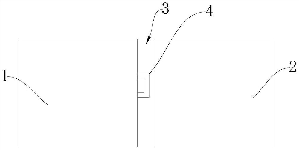
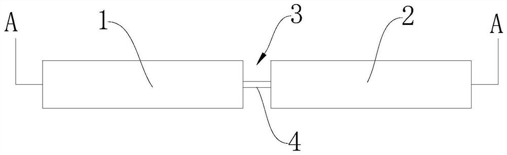
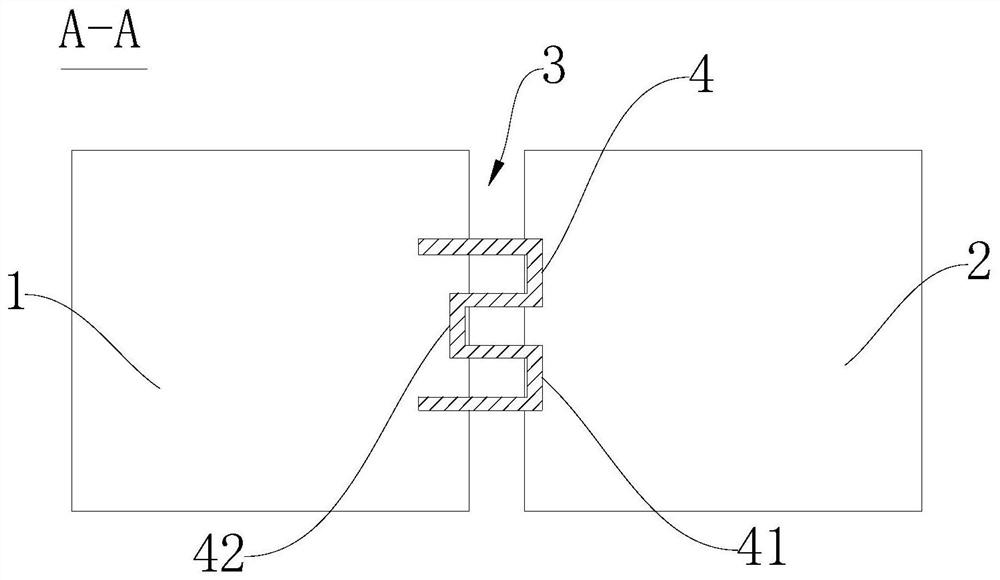
[0043] Such as figure 2 with image 3 Shown is a schematic diagram of the metal wire structure provided by the first embodiment of the present invention, such as image 3 As shown, the metal wire 4 includes a first metal wire, the first metal wire vertically crosses the scribe groove 3 between the first chip 1 and the second chip 2, and the two connecting ends of the first metal wire They are all located in the first chip 1, and the connection terminals are used to connect the test circuit modules in the chip.

[0044] In this embodiment, the first metal wire is a bow-shaped metal wire, the first metal wire has a rectangular wavy structure with one trough 42 and two crests 41, and the trough 42 of the first metal wire is located at the second In one chip 1 , two peaks 41 are located in the second chip 2 .

[0045] In this embodiment, the metal wires are copper wires.

[0046] In this embodiment, the metal wire 4 is arranged between the first chip 1 and the second chip 2 i...

Embodiment 2

[0057] Such as Figure 5 with Image 6 Shown is a schematic structural diagram of the metal wire 4 provided by the second embodiment of the present invention, as Image 6 As shown, the metal wire 4 includes a first metal wire, the first metal wire vertically crosses the scribe groove 3 between the first chip 1 and the second chip 2, and the two connecting ends of the first metal wire They are all located in the first chip 1, and the connection terminals are used to connect the test circuit modules in the chip.

[0058] In this embodiment, the first metal wire is a bow-shaped metal wire, and the first metal wire has a rectangular wavy structure with one trough 42 and two crests 41, and the troughs 42 of the first metal wire are located at In the first chip 1 , two peaks 41 are located in the second chip 2 .

[0059] In this embodiment, the metal wire 4 is arranged between the first chip 1 and the second chip 2 in a vertical arc shape.

[0060] In this embodiment, the two co...


PUM


Abstract

The invention provides a chip metal wire, a manufacturing method thereof and a wafer, and belongs to the field of chips. The chip metal wire comprises a first metal wire, wherein the first metal wire vertically crosses a scribing groove between two adjacent chips, two connecting ends of the first metal wire are located in the same chip, and the connecting ends are used for connecting a test circuit module in the chip. According to the chip metal wire provided by the invention, the chip metal wire vertically crosses the scribing groove between the two adjacent chips, so that the material composition in the scribing groove is kept uniform, the pressures on the two surfaces of the saw blade in the scribing groove are consistent, the cutting quality cannot be influenced by the cutting deflection of the saw blade, and meanwhile, the first metal wire is ensured to be cut by the saw blade.

Description

technical field [0001] The invention relates to the chip field, in particular to a chip metal wire, a chip metal wire manufacturing method and a wafer. Background technique [0002] Wafer dicing (that is, cutting) is an essential process in the semiconductor chip manufacturing process, and it is a post-process in wafer manufacturing. Divide the whole wafer of finished chips into single chips (grains) according to the chip size, which is called wafer dicing. [0003] In the industry, the existing die sawing (that is, scribing) adopts saw blade cutting and laser cutting. Diamond saw blade (grinding wheel) cutting is a traditional scribing method with low cost and occupies a large share of the global chip cutting market. Laser cutting is a new type of scribing method, which can perform non-contact processing, does not generate mechanical stress on the wafer, and has less damage, but the cost is high. [0004] In chip design, the fuse (also known as metal wire, fuse) is used ...

Claims


Application Information

Patent Timeline
Patent Type & Authority Applications(China)
IPC IPC(8): H01L23/58H01L21/66
CPCH01L23/585H01L22/32
Inventor 张贺丰林杰李建强李延王文赫
Owner BEIJING SMARTCHIP MICROELECTRONICS TECH COMPANY
Why Eureka
Try Eureka