Electrode with transparent series resistance for uniform switching of optical modulation devices

a technology of optical modulation device and transparent series resistance, which is applied in the field of devices, can solve the problems of reducing the maximum optical transmission of the device and/or unacceptably increasing the voltage required for switching, and achieve the effects of increasing the reflectance, decreasing the transmission of the device, and increasing the reflectan

Inactive Publication Date: 2008-01-08
TELEDYNE SCI & IMAGING
View PDF16 Cites 52 Cited by
  • Summary
  • Abstract
  • Description
  • Claims
  • Application Information

AI Technical Summary

Benefits of technology

[0015]In one embodiment, the resistive layer within the electrode is of substantially uniform thickness and composition and improves the switching uniformity of the device by increasing the effective resistance between the electrodes, via the cross-film resistance of the resistive layer, so that the effects of the electrode sheet resistances on the inter-electrode voltage distribution are reduced. Preferably, the thickness and composition of the resistive layer are selected to provide the highest cross-film resistance compatible with the required optical and switching characteristics of the device. In particular, an excessively thick resistive layer may significantly reduce the maximum optical transmission of the device and / or unacceptably increase the voltage required for switching.
[0017]The invention further provides a reversible electrochemical mirror (REM) device employing at least one electrode with a resistive innerlayer to improve switching uniformity of the device. The resistive electrode innerlayer is preferably incorporated in a dot matrix counter electrode, but may also be incorporated in a mirror electrode or in both electrodes of the device. In a preferred embodiment, the REM counter electrode is a dot matrix electrode comprising an underlayer of conductive ITO or FTO (preferably 10-20 ohms / square) on a glass or plastic substrate, an innerlayer of a wide-bandgap metallic oxide (Al2O3 or SiO2 or TiO2, for example), and a thin overlayer of ITO or FTO (preferably 100-500 Å thick) with a dot matrix of platinum spheroids deposited thereupon.
[0019]Switching of this preferred REM device involves application of a voltage between the two electrodes. Application of a negative voltage to the mirror electrode relative to the dot matrix electrode tends to cause the electrodepositable metal to dissolve from the dot matrix electrode and to deposit as a mirror layer on the mirror electrode, increasing the reflectance and decreasing the transmission of the device for electromagnetic radiation. Application of a positive voltage to the mirror electrode tends to cause the electrodepositable metal to deposit on the noble metal spheroids of the dot matrix electrode and to dissolve from the mirror electrode, decreasing the reflectance and increasing the transmission of the device. Voltage losses associated with electrode sheet resistances tend to reduce the inter-electrode voltage at locations away from the bus bars, resulting in thinner mirror layers and reduced optical reflectance toward the center of the device. This effect is reduced by the cross-film resistance of the resistive innerlayer, which is electrically in series with the constituent elements of the electrode sheet resistances. For a sufficiently large cross-film resistance, voltage losses associated with the electrode sheet resistances are relatively small so that mirror layer deposits, and the associated reflectance, are substantially uniform across the device.
[0020]The electrode of the invention provides improved switching uniformity for optical modulation devices. It is particularly useful for large-area devices, such as smart windows, but may also be used with other optical modulation devices, including display devices and beam steering devices, including optical shutters. The invention may be applied to optical modulation devices based on various technologies, including reversible metal electrodeposition, electrochromics, organic light emitting diodes, suspended particles, and liquid crystals.

Problems solved by technology

In particular, an excessively thick resistive layer may significantly reduce the maximum optical transmission of the device and / or unacceptably increase the voltage required for switching.

Method used


Image

  • Electrode with transparent series resistance for uniform switching of optical modulation devices
  • Electrode with transparent series resistance for uniform switching of optical modulation devices
  • Electrode with transparent series resistance for uniform switching of optical modulation devices

Examples


example 1

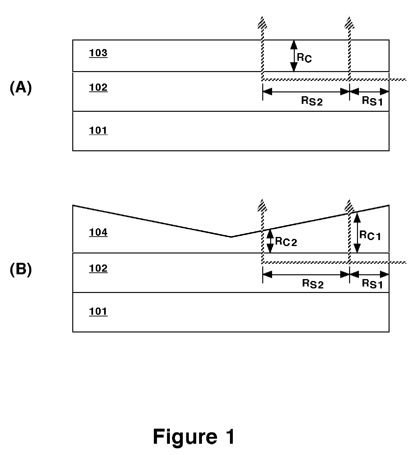
[0042]The electrode resistance increase associated with the sputtered ZnO, SnO2, TiO2 and Al2O3 innerlayers (sandwiched between an 20-ohm ITO underlayer and a 100-ohm ITO / Pt overlayer) was determined by cyclic voltammetry at 50 mV / s between −0.1 and +0.2 V vs. Ag wire reference electrode in a deaerated electrolyte suitable for REM devices (1.5 M AgI and 2.0 M LiBr in gamma-butyrolactone solvent). Electrode resistance was determined from the voltammetric slopes in the cathodic region since those in the anodic region tended to be more variable and somewhat lower, presumably due to greater concentration polarization. Table 1 summarizes the data for the total electrode resistance and the innerlayer resistance (total resistance minus the resistance measured for the ITO / Pt substrate). The values given are the average of two measurements, which generally yielded comparable results. The highest innerlayer resistance (around 300 ohms / cm2) was attained with the thicker TiO2 and Al2O3 innerlay...

example 2

[0044]The densities and diameters of Pt spheroids obtained after plating for 5 minutes at −0.45 V vs. SCE from a commercial Pt plating bath (Technic, Inc., Platinum-A bath) operated at pH 11.5 and 80° C. were determined from scanning electron micrographs for ITO / SnO2 specimens, with and without an ITO overlayer. Plating on 10-20 ohm / square ITO films without resistive innerlayers under the same conditions consistently gave 1-3 million spheroids / cm2 with diameters of 1.2-1.3 μm. Plating directly on the thin SnO2 layers gave very low Pt spheroid densities. In all cases, plating on the specimens with ITO surface modifications on SnO2 innerlayers gave Pt spheroid diameters and densities within the ranges obtained for specimens without the resistive innerlayers, indicating that the electrochemical properties of sputtered ITO were not affected by the resistive innerlayers.


PUM

PropertyMeasurementUnit
sheet resistancesaaaaaaaaaa
sheet resistanceaaaaaaaaaa

Abstract

Switching uniformity of an optical modulation device for controlling the propagation of electromagnetic radiation is improved by use of an electrode comprising an electrically resistive layer that is transparent to the radiation. The resistive layer is preferably an innerlayer of a wide-bandgap oxide sandwiched between layers of indium tin oxide or another transparent conductor, and may be of uniform thickness, or may be graded so as to provide further improvement in the switching uniformity. The electrode may be used with electrochromic and reversible electrochemical mirror (REM) smart window devices, as well as display devices based on various technologies.

Description

GOVERNMENT RIGHTS[0001]This invention was made with Government support under Contract No. DE-FC26-03NT41951 awarded by the Department of Energy. The Government has certain rights in this invention.CROSS-REFERENCE TO RELATED APPLICATIONS[0002]This application is related to U.S. Pat. Nos. 5,903, 382; 5,923,456; 6,111,685; 6,166,847; 6,256,135; 6,301,039; 6,400,491; 6,552,843; 6,721,080 and 6,798,556; and to U.S. patent application, Ser. No. 10 / 211,494, filed Aug. 1, 2002 (entitled “Locally-Distributed Electrode and Method of Fabrication”), now U.S. Pat. No. 7,022,210, all of which are assigned to the assignee of the present application. The teaching of each of these patents and patent applications is incorporated herein by reference.[0003]1. Field of the Invention[0004]This invention is concerned with devices, such as smart windows and optical attenuators, for controlling the propagation of electromagnetic radiation.[0005]2. Description of the Related Art[0006]Smart windows are design...

Claims


Application Information

Patent Timeline
Patent Type & Authority Patents(United States)
IPC IPC(8): G02F1/15G02F1/00G02F1/153H01L21/00G02F1/1506
CPCG02F1/1506G02F1/155G02F1/13439
Inventor TENCH, D. MORGANCUNNINGHAM, MICHAEL A.KOBRIN, PAUL H.
Owner TELEDYNE SCI & IMAGING
Why Eureka
Try Eureka