Semiconductor device and preparation method thereof

A semiconductor and device technology, applied in the field of semiconductor devices and their preparation

Pending Publication Date: 2021-09-10
INST OF MICROELECTRONICS CHINESE ACAD OF SCI
View PDF3 Cites 0 Cited by
  • Summary
  • Abstract
  • Description
  • Claims
  • Application Information

AI Technical Summary

Problems solved by technology

[0003] The embodiment of the present application provides a semiconductor device and its preparation method, which solves the technical problem of mechanically re

Method used


Image

  • Semiconductor device and preparation method thereof
  • Semiconductor device and preparation method thereof
  • Semiconductor device and preparation method thereof

Examples


Embodiment 1

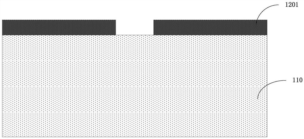
[0027] Such as figure 1 As shown, a method for preparing a semiconductor device is provided, including: providing a layer to be filled 110; forming a patterned mask layer on the upper surface of the layer to be filled 110, and etching the layer to be filled 110 based on the mask layer to form a layer to be filled. Filling the pattern; forming a filling layer 140 in the pattern to be filled and on the upper surface of the mask layer; using the mask layer as an etching barrier layer to etch the filling layer 140 so that the filling layer 140 is flush with the surface of the mask layer; removing the mask layer.

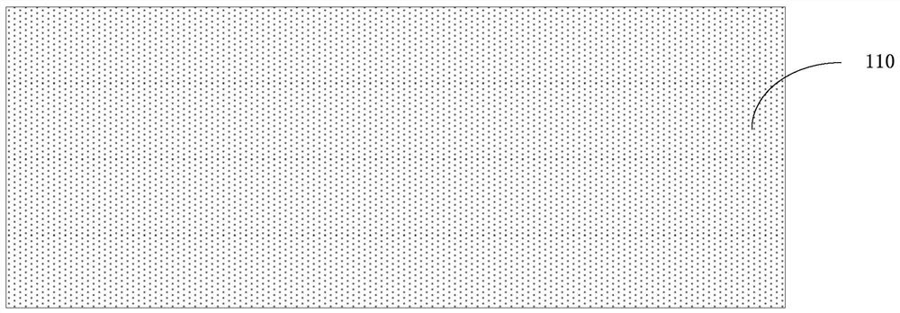
[0028] S110: providing the layer 110 to be filled, such as figure 2 shown.

[0029] In one embodiment, the layer to be filled 110 includes a dielectric layer.

[0030] In one embodiment, the dielectric layer includes silicon dioxide or a low dielectric constant material.

[0031] In one embodiment, step S110 includes:

[0032] S1101: providing a substrate;

[0033...

Embodiment 2

[0078] Such as Figure 8 As shown, a semiconductor device is provided, including: a layer to be filled 110, the layer to be filled 110 has a pattern to be filled; a patterned mask layer, located on the upper surface of the layer to be filled, the patterned mask layer exposes the layer to be filled Pattern; filling layer 140, located in the pattern to be filled, and the filling layer 140 is flush with the surface of the mask layer.

[0079] In one embodiment, the pattern to be filled includes a first pattern to be filled 1301 and a second pattern to be filled 1302 interconnected, the first pattern to be filled 1301 includes a through hole, and the second pattern to be filled 1302 includes a trench.

[0080] In one embodiment, the layer to be filled 140 includes a dielectric layer, the filling layer 140 includes a metal layer, and the metal layer includes ruthenium or cobalt.

[0081] In one embodiment, the dielectric layer includes silicon dioxide or a low dielectric constant ...


PUM


Abstract

The invention discloses a semiconductor device and a preparation method thereof. The preparation method of the semiconductor device comprises the following steps: providing a to-be-filled layer; forming a patterned mask layer on the upper surface of the to-be-filled layer, and etching the to-be-filled layer based on the mask layer to form a to-be-filled pattern; forming a filling layer in the to-be-filled pattern and on the upper surface of the mask layer; etching the filling layer by taking the mask layer as an etching barrier layer, so that the filling layer is flush with the surface of the mask layer; and removing the mask layer. The mask layer is used as the etching barrier layer to etch the filling layer, so that the filling layer is flush with the surface of the mask layer, the redundant filling layer can be prevented from being removed in a mechanical mode, and defects are avoided.

Description

technical field [0001] The invention relates to the field of semiconductors, in particular to a semiconductor device and a preparation method thereof. Background technique [0002] Integrated circuits include many connected structures. Generally, the connected structures are formed by Damascene technology, but the inventors of the present application have found that the above-mentioned technology has at least the following technical problems: it is easy to form defects on the connected structures, which affects the stability and yield of devices, and increases production. cost. Contents of the invention [0003] The embodiment of the present application provides a semiconductor device and a manufacturing method thereof, which solves the technical problem of defects caused by mechanically removing redundant filling layers in the prior art, and achieves the technical effects of reducing device defects and increasing device stability. [0004] The present invention provides ...

Claims


Application Information

Patent Timeline
IPC IPC(8): H01L21/768H01L21/027H01L23/532
CPCH01L21/76877H01L21/0274H01L23/53242H01L23/53209
Inventor 孙祥烈许静罗军赵超
Owner INST OF MICROELECTRONICS CHINESE ACAD OF SCI
Why Eureka
Try Eureka