Semiconductor structure and forming method thereof

A technology of semiconductor and channel structure, which is applied in semiconductor devices, semiconductor/solid-state device manufacturing, transistors, etc., can solve the problems of difficult channel and poor control ability of gate structure to channel, so as to improve performance and performance The effect of uniformity

Pending Publication Date: 2021-09-28
SEMICON MFG INT (SHANGHAI) CORP +1
View PDF0 Cites 0 Cited by
  • Summary
  • Abstract
  • Description
  • Claims
  • Application Information

AI Technical Summary

Problems solved by technology

However, as the channel length of the device is shortened, the distance between the source and the drain of the device is also shortened, so the ability of the gate structure to control the channel becomes worse, and the gate voltage pinches off the channel. The difficulty of the channel is also increasing, making the phenomenon of subthreshold leakage (subthreshold leakage), the so-called short-channel effect (short-channel effects, SCE) more prone to occur

Method used


Image

  • Semiconductor structure and forming method thereof
  • Semiconductor structure and forming method thereof
  • Semiconductor structure and forming method thereof

Examples


Embodiment Construction

[0020] Currently formed devices still suffer from poor performance. The reasons for the poor performance of the device are analyzed in conjunction with a method of forming a semiconductor structure.

[0021] refer to Figure 1 to Figure 3 , is a structural schematic diagram corresponding to each step in a method for forming a semiconductor structure.

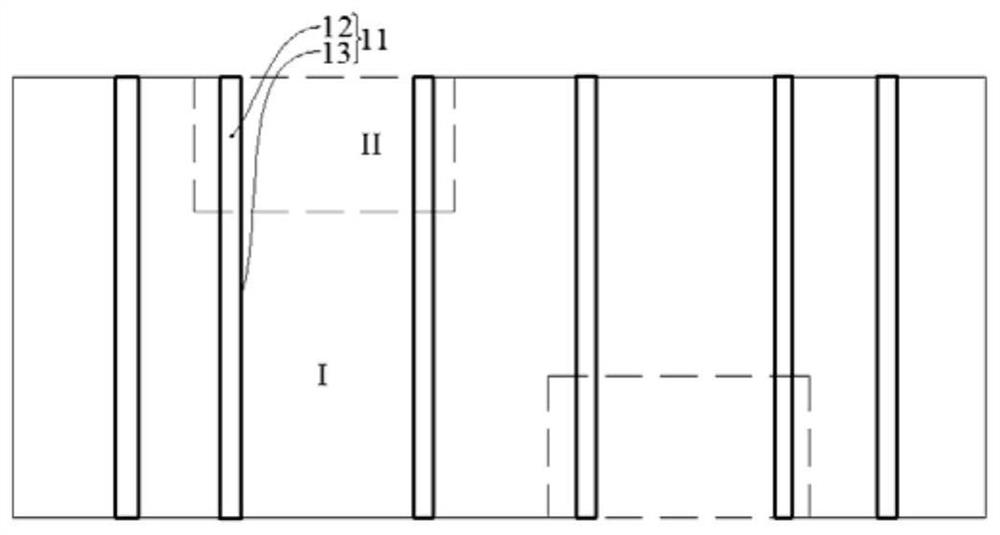
[0022] Such as figure 1 As shown, a base is provided, and the base includes a device region I (the area in the thin solid line frame in the figure) and an isolation area II (the area in the dotted line frame in the figure), and the base includes the substrate and is separated from the substrate. The plurality of fins 11 in the isolation region II are dummy fins 12 , and the fins 11 in the device region I are device fins 13 .

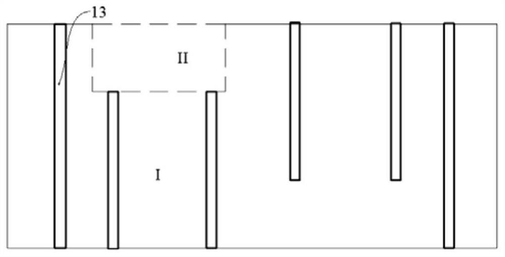
[0023] Such as figure 2 As shown, the dummy fins 12 in the isolated region II are removed.

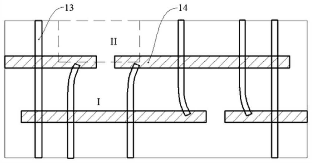
[0024] Such as image 3 As shown, a dummy gate structure 14 is formed across the device fin 13, and the d...


PUM


Abstract

The invention discloses a semiconductor structure and a forming method thereof, and the forming method comprises the steps: providing a substrate which comprises a substrate and a plurality of channel structures located on the substrate, wherein the substrate comprises a device region and an isolation region which are adjacent to each other, the channel structure located in the isolation region is a pseudo channel structure, and the channel structure located in the device region is a device channel structure; forming an initial gate structure crossing the channel structure; and etching the channel structure at the junction of the isolation region and the device region and the initial gate structure intersected with the channel structure at the junction to form an opening for disconnecting the channel structure and the initial gate structure. In the embodiment of the invention, the formation steps of the gate structure generally comprise: forming the gate material layer on the substrate, etching the gate structure material layer, and forming the initial gate structure, wherein the pattern density of the channel structure of the isolation region and the device region is more uniform, so the probability that the channel structure is bent or inclined is lower, and the performance and the performance uniformity of the device can be improved.

Description

technical field [0001] Embodiments of the present invention relate to the field of semiconductor manufacturing, and in particular, to a semiconductor structure and a method for forming the same. Background technique [0002] In semiconductor manufacturing, with the development trend of ultra-large-scale integrated circuits, the feature size of integrated circuits continues to decrease. In order to adapt to smaller feature sizes, metal-oxide-semiconductor field-effect transistors (Metal-Oxide-Semiconductor Field-Effect Transistor , MOSFET) channel length has been shortened accordingly. However, as the channel length of the device is shortened, the distance between the source and the drain of the device is also shortened, so the ability of the gate structure to control the channel becomes worse, and the gate voltage pinches off the channel. The channel becomes more and more difficult, making subthreshold leakage (subthreshold leakage), the so-called short-channel effect (shor...

Claims


Application Information

Patent Timeline
Patent Type & Authority Applications(China)
IPC IPC(8): H01L21/8234H01L21/8244H01L27/088H01L27/11
CPCH01L21/823412H01L21/823431H01L21/823481H01L21/823437H01L27/0886H10B99/00H10B10/12
Inventor 王楠
Owner SEMICON MFG INT (SHANGHAI) CORP
Why Eureka
Try Eureka