Method for preparing Raman substrate by using structured probe

A Raman-based and structured technology, applied in Raman scattering, material excitation analysis, instruments, etc., can solve the problems of uneven distribution of "hot spots", affecting Raman detection results, and fewer types of processed materials, etc., to achieve Raman Enhances good results, eliminates alignment issues, highly reproducible results

Inactive Publication Date: 2021-10-01
HARBIN INST OF TECH
View PDF8 Cites 0 Cited by
  • Summary
  • Abstract
  • Description
  • Claims
  • Application Information

AI Technical Summary

Problems solved by technology

Nanoparticles prepared by chemical synthesis have problems of consistency, poor repeatability, uneven density distribution, and difficult structure control, which will lead to uneven distribution of "hot spots" and affect Raman detection results
High-resolution nanostructures can be prepared by nanofabrication technology, but the cost is high, the types of processing materials are small, and the processing efficiency is low.

Method used


Image

  • Method for preparing Raman substrate by using structured probe
  • Method for preparing Raman substrate by using structured probe
  • Method for preparing Raman substrate by using structured probe

Examples


Embodiment Construction

[0021] The technical solution of the present invention will be further described below in conjunction with the accompanying drawings, but it is not limited thereto. Any modification or equivalent replacement of the technical solution of the present invention without departing from the spirit and scope of the technical solution of the present invention should be covered by the present invention. within the scope of protection.

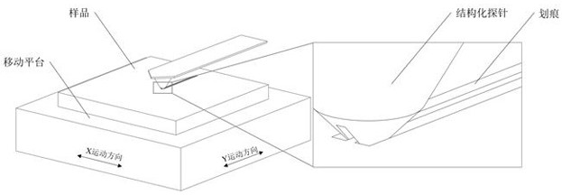
[0022] The invention provides a method for preparing a Raman substrate by using a structured probe. The method mainly uses a structured probe to achieve SERS with good structural stability, high sensitivity and good repeatability through a simple scribing method. Substrate preparation. Specific steps are as follows:

[0023] Step 1. Structured probe preparation

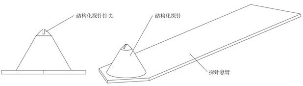
[0024] (1) The structured probe is designed according to the shape of the diamond probe, and its structure is mainly composed of the probe cantilever, the probe and the structured tip, such a...


PUM


Abstract

The invention discloses a method for preparing a Raman substrate by using a structured probe, and the method comprises the following steps: 1, processing a tip of a diamond probe by using an FIB technology, and modifying the diamond probe into a structured diamond probe with a gap; and 2, mounting the structured probe prepared in the step 1 on an AFM processing system, pressing the structured probe into the surface of a sample with a constant normal load, and controlling a processing track through a motion platform, so that the structured probe is subjected to multiple times of scribing under a standard feed rate, and a nano-structure array is processed. According to the method, the structured probe is adopted to prepare the substrate, two paths of nano grooves can be processed after one-time scribing, and compared with a single-tip probe, the efficiency of the method for preparing the substrate by adopting the structured probe is higher. The probe provided by the invention is processed by utilizing an existing probe, compared with the original probe, the probe has a smaller processing size, a smaller nano structure can be processed under a given load, a gap between adjacent structures is smaller, and the Raman enhancement effect is better.

Description

technical field [0001] The invention belongs to the technical field of Raman substrate preparation, and relates to a method for preparing a surface-enhanced Raman substrate based on AFM processing. Background technique [0002] As a label-free detection method, Raman detection has the advantages of high detection sensitivity, low detection cost and simple detection method by detecting selected molecules through specific interaction sites. Micro-nanostructured surfaces can be used as surface-enhanced Raman scattering (SERS) substrates, which have broad application prospects in the detection of biomolecules, flammables and toxic pesticides. [0003] The current methods for preparing SERS substrates mainly include chemical synthesis and nanofabrication. Nanoparticles prepared by chemical synthesis have problems of consistency, poor repeatability, uneven density distribution, and difficult structure control, which will lead to uneven distribution of "hot spots" and affect Raman...

Claims


Application Information

Patent Timeline
Patent Type & Authority Applications(China)
IPC IPC(8): G01N21/65
CPCG01N21/658
Inventor 耿延泉李子翰刘宇闫永达赵学森
Owner HARBIN INST OF TECH
Why Eureka
Try Eureka