Check patentability & draft patents in minutes with Patsnap Eureka AI!

Semiconductor structure and preparation method thereof

A semiconductor and bit line technology, applied in the field of semiconductor structure and its preparation, can solve problems such as bit line tilt and collapse

Active Publication Date: 2021-10-01
CHANGXIN MEMORY TECH INC
View PDF8 Cites 1 Cited by
  • Summary
  • Abstract
  • Description
  • Claims
  • Application Information

AI Technical Summary

Problems solved by technology

[0004] Based on this, it is necessary to provide a semiconductor structure and its preparation method for the problem that the tension can easily cause the bit line to tilt and collapse during wet cleaning.

Method used


Image

  • Semiconductor structure and preparation method thereof
  • Semiconductor structure and preparation method thereof
  • Semiconductor structure and preparation method thereof

Examples


Embodiment Construction

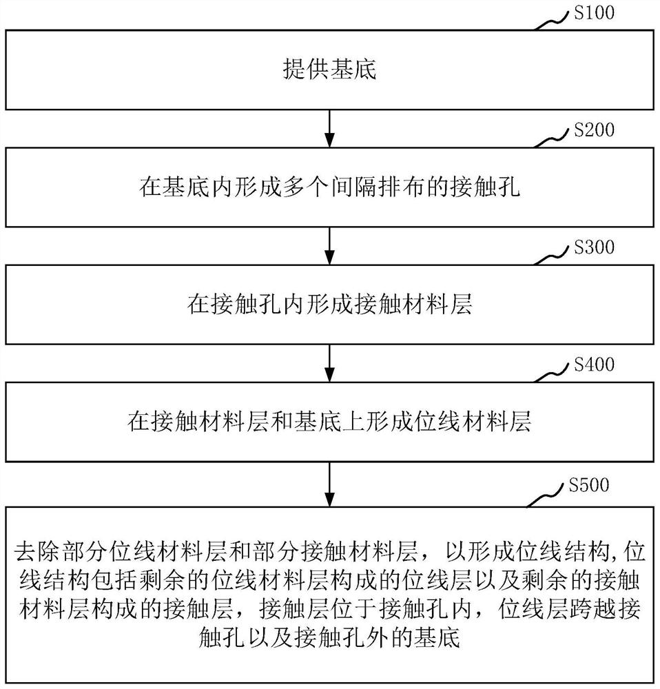
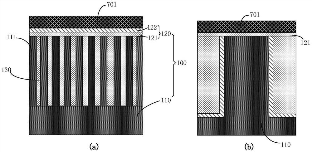
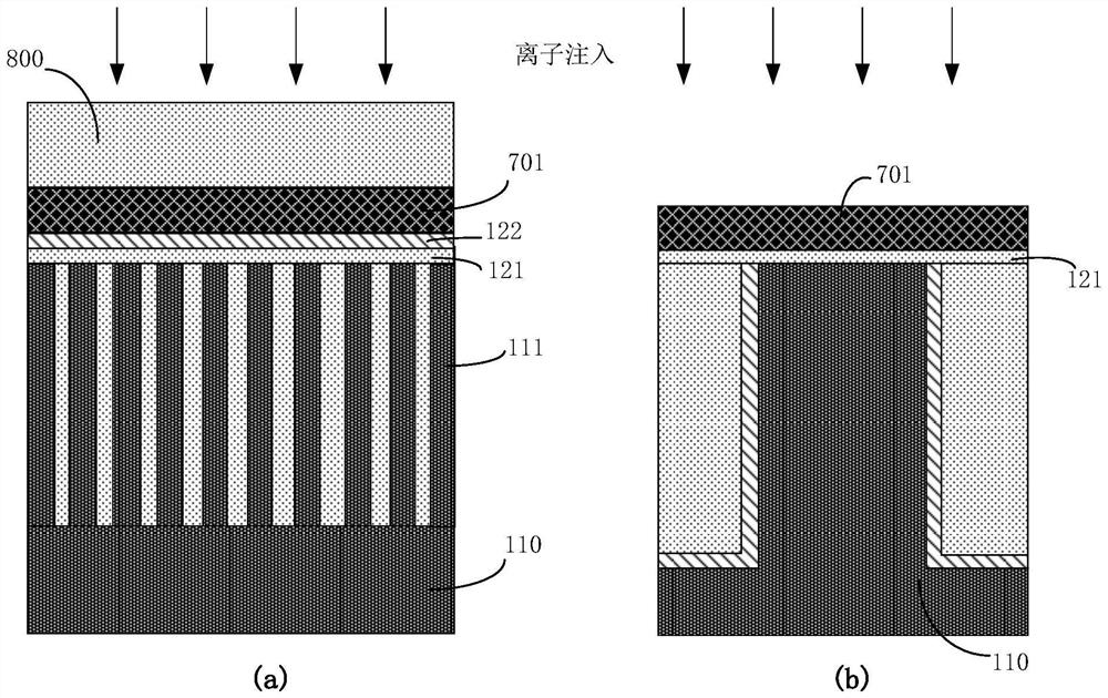
[0064] In order to facilitate the understanding of the present invention, the present invention will be described more fully below with reference to the associated drawings. Preferred embodiments of the invention are shown in the drawings. However, the present invention can be embodied in many different forms and is not limited to the embodiments described herein. On the contrary, the purpose of providing these embodiments is to make the disclosure of the present invention more thorough and comprehensive.

[0065] It should be noted that when an element is referred to as being “fixed” to another element, it can be directly on the other element or there can also be an intervening element. When an element is referred to as being "connected to" another element, it can be directly connected to the other element or intervening elements may also be present. As used herein, the terms "vertical", "horizontal", "left", "right", "upper", "lower", "front", "rear", "circumferential" and...


PUM


Abstract

The invention relates to a semiconductor structure and a preparation method thereof. The preparation method of the semiconductor structure comprises the steps of providing a substrate; forming a plurality of contact holes arranged at intervals in the substrate; forming a contact material layer in the contact hole; forming a bit line material layer on the contact material layer and the substrate; and removing part of the bit line material layer and part of the contact material layer to form a bit line structure, wherein the bit line structure comprises a bit line layer formed by the remaining bit line material layer and a contact layer formed by the remaining contact material layer, the contact layer is located in the contact hole, and the bit line layer crosses the contact hole and the substrate outside the contact hole. According to the invention, the height of the bit line structure can be effectively reduced, so that the bit line structure is effectively prevented from inclining or collapsing in the subsequent manufacturing process.

Description

technical field [0001] The invention relates to the technical field of semiconductors, in particular to a semiconductor structure and a preparation method thereof. Background technique [0002] In the manufacturing process of semiconductor memory devices, bit lines are usually formed by dry etching. After the bit lines are formed by dry etching, a series of organic substances caused by dry etching can be removed by wet cleaning. [0003] However, during wet cleaning, there will be tension between the bit lines due to the flow of the solution. Tension can easily cause the bit line to tilt and collapse. Contents of the invention [0004] Based on this, it is necessary to provide a semiconductor structure and a preparation method thereof for the problem that the bit line is easily tilted and collapsed due to tension during wet cleaning. [0005] A method for preparing a semiconductor structure, comprising: [0006] provide the basis; [0007] forming a plurality of conta...

Claims


Application Information

Patent Timeline
Patent Type & Authority Applications(China)
IPC IPC(8): H01L21/8242H01L21/768H01L23/48H01L27/108H10B12/00
CPCH01L21/76805H01L21/76895H01L23/481H10B12/30H10B12/485H10B12/482
Inventor 孔忠洪海涵
Owner CHANGXIN MEMORY TECH INC
Features
  • R&D
  • Intellectual Property
  • Life Sciences
  • Materials
  • Tech Scout
  • Unparalleled Data Quality
  • Higher Quality Content
  • 60% Fewer Hallucinations
Learn More