Solar cell grid line structure and solar cell using the same

A solar cell and wire structure technology, applied in the field of solar cells, can solve the problems of immaturity of silver-coated copper, inability to discharge directly, and high processing cost, and achieve the effects of reducing preparation cost, ensuring efficiency, and reducing consumption of silver paste

Pending Publication Date: 2021-10-01
TRINASOLAR CO LTD
0 Cites 1 Cited by

AI-Extracted Technical Summary

Problems solved by technology

Other methods of preparing electrodes include electroplating and silver-coated copper particles. However, electrodes prepared by electroplating are generally composed of Ni/Cu/Ag, which can reduce the consumption of silver. However, electroplating will produce a larg...

Method used

[0030] As shown in FIG. 1, it is a schematic diagram of a solar cell grid wire structure 10 in the prior art. According to FIG. 1, the grid line structure 10 has two adjacent main grid lines 111 and 112, and between the two main grid lines 111 and 112, there are a plurality of thin grid lines 12, the above-mentioned main grid lines and thin grid lines They are all arranged on a silicon chip (in order to keep the drawing simple, the silicon chip is not shown in FIG. 1 ). On this basis, there is also an "H"-shaped line 13 between every two thin grid lines 12 to connect two adjacent thin grid lines 12 . As mentioned above, although the photoelectric conversion efficiency of the solar cell can be guaranteed by adopting the grid wire structure 10 shown in Figure 1, a large amount of silver is required to prepare a plurality of grid wires, especially a p...

Abstract

The invention provides a solar cell grid line structure and a solar cell using the same, the solar cell grid line structure comprises a plurality of main grid lines which extend along a first direction and are arranged at intervals along a second direction, and a plurality of thin grid lines which extend along the second direction and are arranged at intervals along the first direction, the first direction is not parallel to the second direction, the plurality of main grid lines are electrically connected with the plurality of thin grid lines respectively, and each thin grid line is provided with a broken section between any two adjacent main grid lines. According to the solar cell grid line structure and the solar cell using the same, the silver paste consumption can be effectively reduced on the basis of ensuring the cell efficiency, and the preparation cost of the solar cell is reduced.

Application Domain

Photovoltaic energy generationSemiconductor devices

Technology Topic

PhysicsElectrical battery +5

Image

  • Solar cell grid line structure and solar cell using the same
  • Solar cell grid line structure and solar cell using the same
  • Solar cell grid line structure and solar cell using the same

Examples

  • Experimental program(1)

Example Embodiment

[0023] In order to more clearly illustrate the technical solutions of the embodiments of the present application, the following briefly introduces the drawings that need to be used in the description of the embodiments. Obviously, the accompanying drawings in the following description are only some examples or embodiments of the present application, and those skilled in the art can also apply the present application to other similar scenarios. Unless otherwise apparent from context or otherwise indicated, like reference numerals in the figures represent like structures or operations.
[0024] As indicated in this application and claims, the terms "a", "an", "an" and/or "the" do not refer to the singular and may include the plural unless the context clearly indicates an exception. Generally speaking, the terms "comprising" and "comprising" only suggest the inclusion of clearly identified steps and elements, and these steps and elements do not constitute an exclusive list, and the method or device may also contain other steps or elements.
[0025] The relative arrangements of components and steps, numerical expressions and numerical values ​​set forth in these embodiments do not limit the scope of the present application unless specifically stated otherwise. At the same time, it should be understood that, for the convenience of description, the sizes of the various parts shown in the drawings are not drawn according to the actual proportional relationship. Techniques, methods and devices known to those of ordinary skill in the relevant art may not be discussed in detail, but where appropriate, such techniques, methods and devices should be considered part of the Authorized Specification. In all examples shown and discussed herein, any specific values ​​should be construed as exemplary only, and not as limitations. Therefore, other examples of the exemplary embodiment may have different values. It should be noted that like numerals and letters denote like items in the following figures, therefore, once an item is defined in one figure, it does not require further discussion in subsequent figures.
[0026] In the description of the present application, it should be understood that orientation words such as "front, back, up, down, left, right", "horizontal, vertical, vertical, horizontal" and "top, bottom" etc. indicate the orientation Or positional relationship is generally based on the orientation or positional relationship shown in the drawings, and is only for the convenience of describing the application and simplifying the description. In the absence of a contrary statement, these orientation words do not indicate or imply the device or element referred to It must have a specific orientation or be constructed and operated in a specific orientation, so it should not be construed as limiting the protection scope of the present application; the orientation words "inner and outer" refer to the inner and outer relative to the outline of each component itself.
[0027] For the convenience of description, spatially relative terms may be used here, such as "on ...", "over ...", "on the surface of ...", "above", etc., to describe the The spatial positional relationship between one device or feature shown and other devices or features. It will be understood that the spatially relative terms are intended to encompass different orientations of the device in use or operation in addition to the orientation depicted in the figures. For example, if the device in the figures is turned over, devices described as "above" or "above" other devices or configurations would then be oriented "beneath" or "above" the other devices or configurations. under other devices or configurations". Thus, the exemplary term "above" can encompass both an orientation of "above" and "beneath". The device may be otherwise oriented (rotated 90 degrees or at other orientations) and the spatially relative descriptions used herein interpreted accordingly.
[0028] In addition, it should be noted that the use of words such as "first" and "second" to define components is only for the convenience of distinguishing corresponding components. To limit the protection scope of this application. In addition, although the terms used in this application are selected from known and commonly used terms, some terms mentioned in the specification of this application may be selected by the applicant according to his or her judgment. described in the relevant section of the description. Furthermore, it is required that this application be understood not only by the actual terms used, but also by the meaning implied by each term.
[0029]It will be understood that when an element is referred to as being "on," "connected to," "coupled to" or "contacting" another element, it can be directly on the other element. On, connected or coupled to, or in contact with, the other component, or there may be an intervening component. In contrast, when an element is referred to as being "directly on," "directly connected to," "directly coupled to" or "directly contacting" another element, there are no intervening elements present. Likewise, when a first component is referred to as being "electrically contacting" or "electrically coupled to" a second component, there exists an electrical path between the first component and the second component that allows electrical current to flow. This electrical path may include capacitors, coupled inductors, and/or other components that allow current to flow, even without direct contact between conductive components.
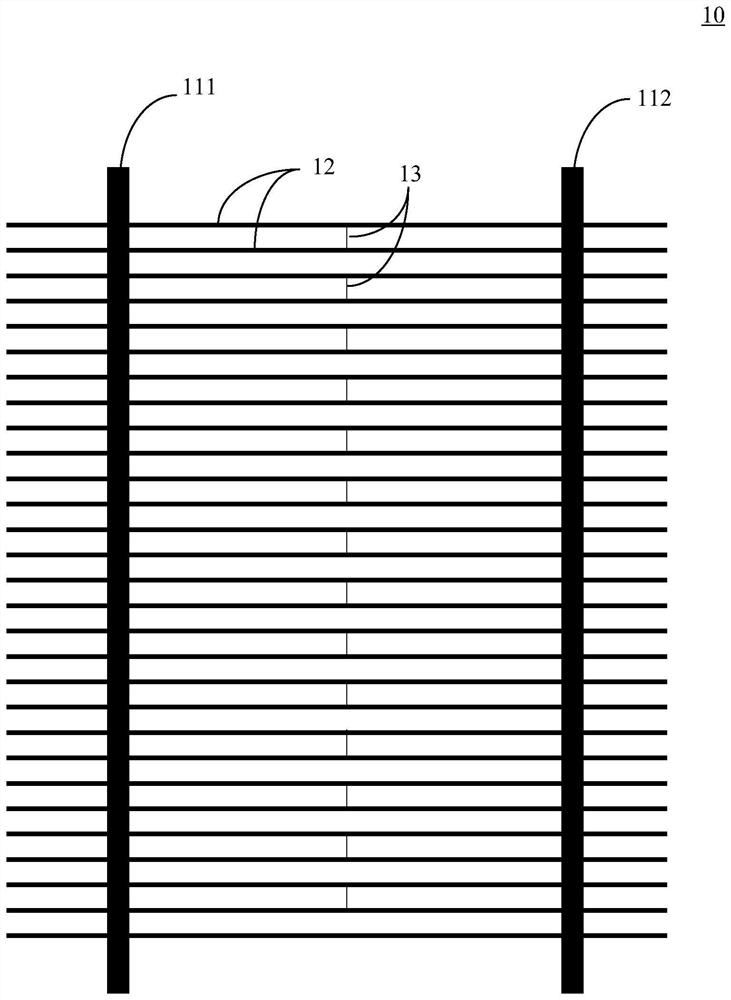
[0030] like figure 1 Shown is a schematic diagram of a solar cell grid wire structure 10 in the prior art. according to figure 1 , the grid line structure 10 has two adjacent main grid lines 111 and 112, and between the two main grid lines 111 and 112, there are a plurality of thin grid lines 12, and the above-mentioned main grid lines and thin grid lines are arranged on the silicon die (to keep the drawing simple, the silicon die is not on the figure 1 shown in ). On this basis, there is also an "H"-shaped line 13 between every two thin grid lines 12 to connect two adjacent thin grid lines 12 . As mentioned above, using the figure 1 Although the grid line structure 10 shown can ensure the photoelectric conversion efficiency of the solar cell, a large amount of silver paste is required to prepare a plurality of grid lines, especially a plurality of thin grid lines 12, which improves the production efficiency of the solar cell. Cost, this is also the problem to be solved by the present invention.
[0031] An embodiment of the present invention proposes a grid wire structure of a solar cell, which can effectively reduce the consumption of silver paste and reduce the manufacturing cost of the solar cell on the basis of ensuring the efficiency of the cell.
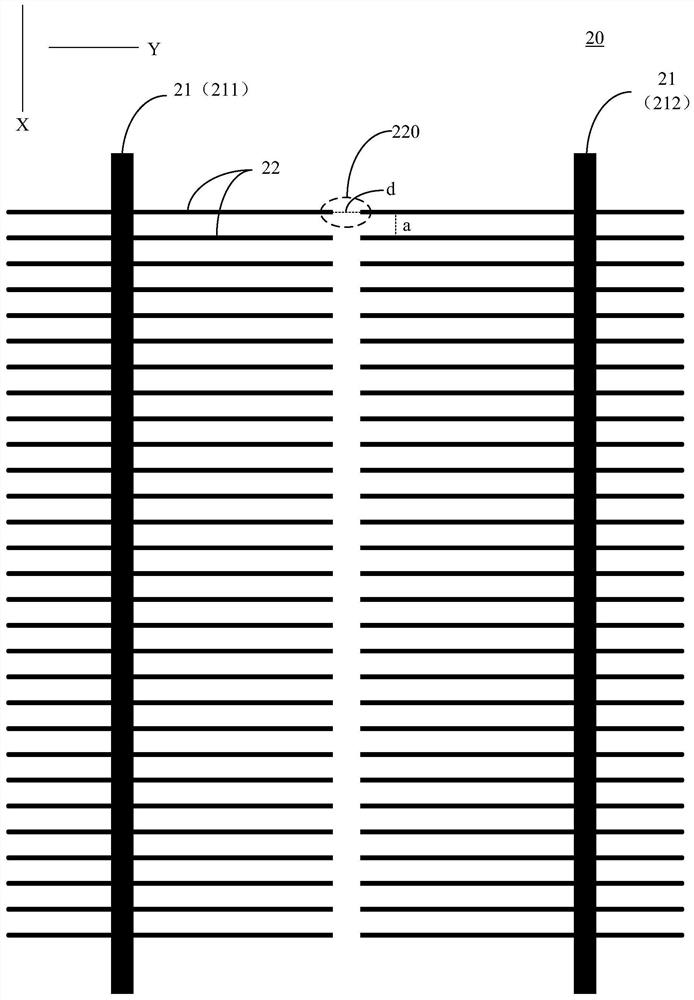
[0032] like figure 2 Shown is a schematic diagram of the grid wire structure 20 of the solar cell in this embodiment. according to figure 2 , the gate line structure 20 includes a plurality of main gate lines 21 extending along the first direction X and arranged at intervals along the second direction Y. figure 2 The two adjacent busbar lines 211 and 212 are shown in .
[0033] On the other hand, the grid line structure 20 further includes a plurality of thin grid lines 22 extending along the second direction Y and arranged at intervals along the first direction X. As shown in FIG. according to figure 2 It can be seen that the first direction X is not parallel to the second direction Y. More specifically, in figure 2 In the illustrated embodiment, the first direction X is perpendicular to the second direction Y, but the invention is not limited thereto. On this basis, a plurality of busbar lines 21 (such as busbar lines 211 and 212 in the figure) are electrically connected to a plurality of thin gridlines 22 respectively.
[0034] In particular, in the present invention such as figure 2 In the illustrated embodiment, between the main grid lines 211 and 212 , each thin grid line 22 has a disconnection section 220 . and figure 1 Compared with the undisconnected grid line structure 10 shown, the disconnected section 220 provided on each thin grid line 22 effectively reduces the consumption of silver paste as a whole and saves the manufacturing cost of the solar cell.
[0035] according to figure 2 , the length of the disconnected segment 220 of each fine grid line in the grid line structure 20 in the second direction Y is the disconnected distance d (ie figure 2 The distance shown by the dotted line in the Y direction). In some embodiments of the present invention, the disconnection distance d is less than or equal to twice the distance a between two adjacent thin grid lines. Adopting such parameter setting can make the grid line structure of the present invention save silver paste consumption. At the same time, the effect on the efficiency of the battery adopting the grid line structure of the present invention is reduced as much as possible.
[0036] Further, considering the appearance of the prepared solar cell and the preparation process, such as figure 2 In the illustrated embodiment, the disconnection distance d of the disconnection section 220 of each fine grid line 22 is equal. Moreover, between the adjacent busbar lines 211 and 212 , the disconnected sections of all the thin grid lines 22 coincide in the first direction X. Referring to FIG.
[0037] However, the present invention does not limit whether the distances between the disconnected sections of the fine grid lines are equal and whether they overlap in the first direction X in all embodiments. For example, in some other embodiments of the present invention, the disconnection sections of all fine grid lines 22 do not overlap or do not completely overlap in the first direction X, and the disconnection distances of each fine grid line are not necessarily equal . Figure 3a ~ Figure 5 Respectively show different situations from incomplete coincidence to non-coincidence, refer to below Figure 3a ~ Figure 5 A description is given for the specific location of the arrangement of the disconnected sections. For illustrative purposes, Figure 3a ~ Figure 5 The case where the break distances d of the break sections are equal is chosen.
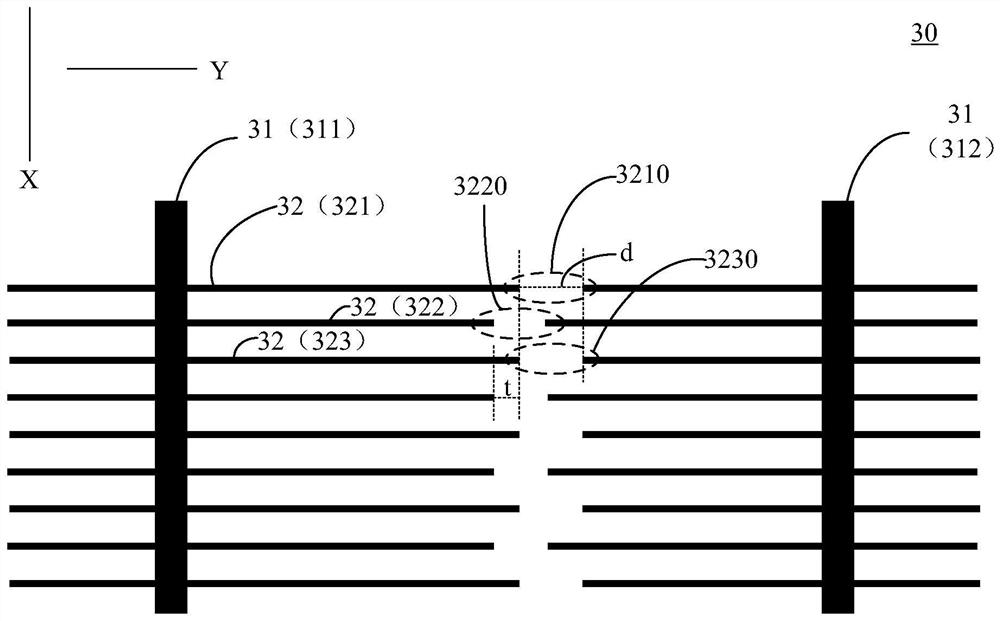
[0038] exist Figure 3a In the illustrated embodiment, the gate line structure 30 has a plurality of main gate lines 31, wherein Figure 3a Shown are two adjacent busbar lines 311 and 312 and a plurality of fine gridlines 32 . Among the plurality of thin grid lines 32 , the thin grid lines 321 and 323 are two odd-numbered thin grid lines. exist Figure 3a , the fine grid lines adjacent to all the odd-numbered fine grid lines are the even-numbered fine grid lines, such as the fine grid line 322 . Moreover, all the odd-numbered thin grid lines and the even-numbered thin grid lines have disconnected sections between the adjacent busbars 311 and 312, for example, the disconnected sections 3210 and 3230 of the odd-numbered thin grid lines 321 and 323 , and the disconnected segment 3220 of the even-numbered fine grid line 322 .
[0039] It can be seen that, with figure 2 Compared with the grid line structure 20 shown, the multiple thin grid lines 32 between two adjacent main grid lines 311 and 312 in the grid line structure 30 also have disconnected sections, but each thin grid line 32 The disconnected sections of are not completely coincident in the first direction X. Specifically, in Figure 3a In the described embodiment, with reference to the auxiliary dotted line in the X direction, the gate line structure 30 is particularly described as a disconnected section (such as the disconnected section 3210) of an odd-numbered thin grid line (such as a thin grid line 321) and an even-numbered thin grid line. The disconnected sections (eg, the disconnected section 3220 ) of the grid lines (eg, the thin grid lines 322 ) do not completely coincide in the first direction X. As shown in FIG.
[0040] To be more specific, as in Figure 3a In the illustrated embodiment, between the adjacent main grid lines 311 and 312, the disconnected section (correspondingly the disconnected area) of any two odd-numbered thin grid lines (for example, the thin grid lines 321 and 323) Sections 3210 and 3230), according to Figure 3a As shown by the dotted line in , overlap in the first direction X. The same, although for the sake of brevity of the drawings in Figure 3a is not clearly marked in , but the disconnected segments of any two even-numbered thin grid lines also coincide in the first direction X. However, the present invention is not limited thereto. For example, in some other embodiments of the present invention, the disconnected sections of any two odd-numbered thin grid lines or any two even-numbered thin grid lines are not in the first direction X. must coincide.
[0041] Finally, about Figure 3a Marks t and d in and Figure 3b This will be described in further detail below.
[0042] Figure 4 Another embodiment of the grid line structure 40 in which the broken sections of the thin grid lines do not overlap is shown. In the gate line structure 40, any two adjacent main gate lines 41 are respectively a first main gate line 411 and a second main gate line 412, between the first main gate line 411 and the second main gate line 412, The disconnected sections of any fine grid lines 42 (for example, the fine grid lines 421 and 422) (for the sake of simplicity of the drawings, in Figure 4 The disconnected section is not specifically shown in the above, you can refer to the above figure 2 and Figure 3a ) The end close to the first main gate line 421 is the first end (the first ends 4211 and 4221 respectively).
[0043] Further, at Figure 4 Among them, the thin grid lines 421 are odd-numbered thin grid lines, and the thin grid lines 422 are even-numbered thin grid lines. The distance between the first end 4211 of the disconnected section of the odd-numbered fine grid line 421 and the first main grid line 411, and the distance between the first end 4221 of the disconnected segment of the even-numbered thin grid line 422 and the first main grid line 411 The difference between them is the stagger distance t. As mentioned above, in Figure 4 In the illustrated embodiment, the disconnection distance d of each fine grid line 42 is equal, and the aforementioned offset distance t is equal to the disconnection distance d. use as Figure 4 The structure shown can achieve better cell efficiency while reducing the consumption of silver paste so as to reduce the manufacturing cost of the solar cell. This effect will be further explained and verified below.
[0044] similarly, due to the Figure 3a In the illustrated embodiment, the disconnected sections of each thin grid line 32 in the grid line structure 30 do not completely overlap in the first direction X, and the odd-numbered thin grid lines (for example, thin grid lines 321) and the even-numbered thin grid lines The serial number thin grid lines (such as the thin grid lines 322) also have a staggered distance t in the first direction X, but in Figure 3a In the illustrated embodiment, the offset distance t is only half of the disconnection distance d.
[0045] Further, in some embodiments of the present invention, such as Figure 3b As shown, in the grid line structure 30', there are odd-numbered thin grid lines 323 and 325 and even-numbered thin grid lines 324 between two adjacent main grid lines 313 and 314. in such as Figure 3b In the illustrated embodiment, there is a stagger distance t between the odd-numbered fine grid line 323 and another odd-numbered thin grid line 325 . The present invention does not limit whether the fine grid lines with the staggered distance are odd-numbered fine grid lines or even-numbered fine grid lines.
[0046] further, Figure 5 An embodiment of the grid line structure 50 in which the disconnected sections of the thin grid lines do not overlap completely in the first direction X is shown. The gate line structure 50 also has a plurality of main gate lines 51, wherein the plurality of thin gate lines 52 between any two main gate lines 511 and 512 have disconnected sections, and Figure 5 In the illustrated embodiment, it is clear that the offset distance t is greater than the break distance d. other about Figure 5 Details of the grid line structure 50 shown can be referred to above for Figure 2 ~ Figure 4 description, which will not be repeated here.
[0047] above reference Figure 2 to Figure 5 The grid line structures 20 to 50 shown are different examples of all the thin grid lines of the present invention being disconnected, and the difference of each grid line structure lies in the position of the disconnected section, and the size between the disconnected section and the stagger distance has a difference. Taking a solar cell with a side length of 158.75mm as an example, only changing the structure of the grid line, as the stagger distance increases, the efficiency first increases and then decreases. Taking the disconnection distance d=2mm as an example, with the change of the stagger distance t ,correspond Figure 2 to Figure 5 The efficiency data of the solar cells prepared by each grid line structure are shown in the following table, and the Baseline in Table 1 is as follows figure 1 The reference structure shown without the fine-grid break:
[0048] group Voc Isc FF Eff Baseline 709.348509 39.192504 82.268551 22.871598 Grid structure 20 710.128805 39.271922 81.745977 22.797419 grid structure 30 710.209291 39.274807 81.800794 22.816968 grid line structure 40 710.171149 39.271922 81.873599 22.834372 grid structure 50 710.176769 39.271922 81.856122 22.829678
[0049] Table 1: Performance comparison of solar cells prepared with different gridline structures
[0050] Among them, Voc is the open circuit voltage, Isc is the short circuit current, FF is the fill factor, and Eff is the photoelectric conversion efficiency. The control conditions for each group are as follows:
[0051] Baseline: d=0, t=0;
[0052] Grid line structure 20: d=2mm, t=0;
[0053] Grid line structure 30: d=2mm, t=1mm;
[0054] Grid line structure 40: d=2mm, t=2mm;
[0055] Grid line structure 50: d=2mm, t=4mm.
[0056] It can be seen that as the stagger distance t increases, the efficiency first increases and then decreases, and when the stagger distance t is just equal to the disconnection distance d, the efficiency is the highest. That is, as mentioned above, Figure 4 The gridline structure 40 shown can have higher efficiency under the same conditions. This preferred efficiency is only as good as figure 1 The difference of the Baseline of the reference case without disconnection shown is less than 0.05%, but the cost of silver consumption can be saved by about 15% when preparing solar cells. It can be seen that, by adopting the grid wire structure of the solar cell of the present invention, the consumption of silver paste can be effectively reduced on the basis of ensuring the efficiency of the cell, thereby reducing the manufacturing cost of the solar cell.
[0057] On the other hand, in order to further confirm the technical effect of the solar cell grid wire structure of the present invention, the comparison between the present invention and the prior art when the fine grid lines are not completely disconnected between any adjacent main grid lines Structure (Baseline) for comparison. When the silver consumption saved by the comparison structure is equal to that of the grid line structure of the present invention, for example, a disconnection distance of the comparison structure is selected to be 2mm, and compared with the structure of the above-mentioned grid line structure 30 of the present invention, that is, d=1mm in the present invention , the case of t=0. Can draw by experimental analysis, the efficiency of the solar cell prepared by grid line structure of the present invention is better than the efficiency of comparison structure, and result is as follows:
[0058] group Voc Isc FF Eff Baseline 709.348509 39.192504 82.268551 22.871598 Structure of the present invention 710.007267 39.244590 82.158923 22.892716 contrast structure 709.923955 39.244590 82.078330 22.867576
[0059] Table 2: Performance Comparison of Solar Cells Prepared by the Grid Wire Structure of the Invention and the Comparative Structure
[0060] From the above description, especially the analysis results of experimental data, it can be seen that the grid wire structure of the solar cell of the present invention can effectively reduce the consumption of silver paste on the basis of ensuring the efficiency of the cell, thereby reducing the production cost of the solar cell. At the same time, compared with other comparative structures with the concept of saving silver paste consumption, the efficiency of the prepared solar cell also has better performance.
[0061] On the basis of the above grid line structure, another aspect of the present invention also proposes a solar cell. The solar cell first includes a basic grid structure, and the basic grid structure is the above-mentioned reference Figure 2 to Figure 5 All the fine grid lines between two adjacent main grid lines illustrated have a grid line structure of a disconnected section. In addition, in some solar cell embodiments of the present invention, the above-mentioned basic grid line structure is also included, and a supplementary grid line structure is also included.
[0062] like Image 6 Shown is a schematic structural diagram of a solar cell 60 according to an embodiment of the present invention. The solar cell 60 has the above-mentioned basic grid line structure and supplementary grid line structure, which are combined below Image 6 Expand the description.
[0063] according to Image 6 , the solar cell 60 has a plurality of busbar lines 61 and a plurality of thin grid lines 62, wherein the three busbar lines arranged in sequence are respectively the first busbar line 611, the second busbar line 612 and the third busbar line line 613. according to Image 6 A first region 601 is formed between the first main gate line 611 and the second main gate line 612 , and a second region 602 is formed between the second main gate line 612 and the third main gate line 613 . In particular, parts of the first main gate line 611 , the second main gate line 612 and the plurality of thin gate lines 62 in the first region 601 have a basic gate line structure 63 . Image 6 The shown basic gate line structure 63 in the first region 601 is specifically the above-mentioned figure 2 The gridline structure 20 shown in . But the present invention is not limited thereto. For example, in some embodiments of the present invention, the basic gate line structure may also be Figure 3a ~ Figure 5 Grid line structures 30-50 shown in .
[0064] Further, at Image 6 Among them, the second busbar 612 , the third busbar 613 and the plurality of thin gridlines 62 in the second region 602 have a supplementary gateline structure 64 . from Image 6 It can be seen that the supplementary gate line structure 64 includes main gate lines 612 and 613 extending along the first direction X and spaced apart along the second direction Y, and extending along the second direction Y and spaced apart along the first direction X A plurality of fine grid lines 62 are arranged. similar in Image 6 Among them, the first direction X and the second direction Y are not parallel, more specifically, they are vertical, but the present invention is not limited thereto.
[0065] Based on such a structure, the main grid lines 612 and 613 are respectively electrically connected to a plurality of thin grid lines 62, and between the two main grid lines 612 and 613, only odd-numbered thin grid lines or only even-numbered thin grid lines Has a disconnected area. exist Image 6 Among them, if the thin grid line 621 is an odd-numbered thin grid line, then the thin grid line 622 is an even-numbered thin grid line. Image 6 In the illustrated embodiment, only the even-numbered thin gridlines in the supplementary gridline structure 64 have the disconnection section 620 .
[0066] in such as Image 6 In the illustrated embodiment, the basic grid line structure 63 and the supplementary grid line structure 64 are arranged at intervals. Understandably, Image 6 What is shown is only a part of the solar cell 60, between any other two main grid lines not shown in the solar cell 60, such as Image 6 A basic gridline structure 63 or a supplementary gridline structure 64 is shown. And, for Image 6 The specific positions of the disconnected sections in the shown basic grid line structure 63 and the supplementary grid line structure 64 are not limited by the present invention.
[0067] from Image 6 The advantage of the solar cell 60 shown in the perspective is that if a battery adopts the basic grid structure, that is, all the thin grid lines between any two main grid lines are disconnected, although the silver consumption can be reduced to a large extent. , but also has certain limitations. Especially in the application scenario of battery testing, the IV and EL test results show that such a fully disconnected design sometimes affects the test results of the battery. Therefore, there are still some limitations in the application process of the solar cell in which all the thin grid lines are disconnected.
[0068] Specifically, when the test probe does not touch the battery or the probe is in poor contact with the battery, obvious black spots will appear in the EL test of the solar cell. These black blocks are mainly due to the design that all the thin grid lines are disconnected so that each main grid line and the thin grid lines connected to it are independent of each other. When it is in contact with the main grid or is in poor contact, the current at this position cannot be effectively transmitted, resulting in a decrease in efficiency during IV testing, or local black spots appearing during EL testing.
[0069] Using the present invention as Image 6 The shown structural design of the basic grid line structure and the supplementary grid line structure arranged at intervals, compared with the battery with all the basic grid line structures, the solar cell 60 has the beneficial effect of saving silver paste consumption, and can further Improvements to the black block problem that may be caused during battery testing.
[0070] In another embodiment of the present invention, as Figure 7 As shown, the solar cell 70 also has a plurality of busbar lines 71 and a plurality of thin grid lines 72, wherein any four busbar lines arranged in sequence are selected as the first busbar line 711, the second busbar line 712, the second busbar line Three main gate lines 713 and a fourth main gate line 714, the first region 701 is formed between the first main gate line 711 and the second main gate line 712, and the first region 701 is formed between the second main gate line 712 and the third main gate line 713 A third region 703 is formed between the second region 702 and the third busbar 713 and the fourth busbar 714 .
[0071] Wherein, parts of the first busbar 711, the second busbar 712, the third busbar 713 and the plurality of thin gridlines 72 in the first region 701 and the second region 702 are supplementary gateline structures 74, which For the specific features of the supplementary gate line structure 74, please refer to the above comparison Image 6 The description of the supplementary gate line structure 64 will not be repeated here. The part of the third busbar 713, the fourth busbar 714, and the plurality of thin gridlines 72 in the third area 703 is the basic gridline structure 73, and the basic gridline structure 73 can also refer to the above reference Figure 2 to Figure 5 description, which will not be repeated here.
[0072] and Image 6 Compared with the illustrated embodiment, the solar cell 70 also has a structural design in which the basic grid structure and the supplementary grid structure are arranged at intervals, but the spacing method is different from that of the solar cell 60 . In the solar cell 70 , every two supplementary gridline structures 74 are followed by a basic gridline structure 73 , which serves as a basic gridline structure combination. while in Image 6 In the solar cell 60 shown, it can be considered that the basic grid line structure is combined into a basic grid line structure 73 followed by a supplementary grid line structure 74 . According to the comparison of the experimental results, compared with Image 6 The shown solar cell 60 and solar cell 70 have a better improvement effect on the black block problem in the battery test application scenario.
[0073] The present invention refers to Figure 2 to Figure 5 The grid line structure can effectively save the consumption of silver paste when preparing solar cells on the basis of ensuring cell efficiency. On this basis, another aspect of the present invention proposes a solar cell, in some embodiments such as Image 6 and Figure 7 As shown, on the basis of ensuring efficiency and saving silver paste consumption, the black block problem in battery test application scenarios can be further improved.
[0074] The basic concepts have been described above, and obviously, for those skilled in the art, the above disclosure of the invention is only an example, and does not constitute a limitation to the present application. Although not expressly stated here, various modifications, improvements and amendments to this application may be made by those skilled in the art. Such modifications, improvements, and amendments are suggested in this application, so such modifications, improvements, and amendments still belong to the spirit and scope of the exemplary embodiments of this application.
[0075] Meanwhile, the present application uses specific words to describe the embodiments of the present application. For example, "one embodiment", "an embodiment", and/or "some embodiments" refer to a certain feature, structure or characteristic related to at least one embodiment of the present application. Therefore, it should be emphasized and noted that two or more references to "an embodiment" or "an embodiment" or "an alternative embodiment" in different places in this specification do not necessarily refer to the same embodiment . In addition, certain features, structures or characteristics of one or more embodiments of the present application may be properly combined.
[0076] In the same way, it should be noted that in order to simplify the expression disclosed in the present application and help the understanding of one or more embodiments of the invention, in the foregoing description of the embodiments of the present application, sometimes multiple features are combined into one embodiment, drawings or descriptions thereof. This method of disclosure does not, however, imply that the subject matter of the application requires more features than are recited in the claims. Indeed, embodiment features are less than all features of a single foregoing disclosed embodiment.
[0077] In some embodiments, numbers describing the quantity of components and attributes are used. It should be understood that such numbers used in the description of the embodiments use the modifiers "about", "approximately" or "substantially" in some examples. grooming. Unless otherwise stated, "about", "approximately" or "substantially" indicates that the stated figure allows for a variation of ±20%. Accordingly, in some embodiments, the numerical parameters used in the specification and claims are approximations that can vary depending upon the desired characteristics of individual embodiments. In some embodiments, numerical parameters should take into account the specified significant digits and adopt the general digit reservation method. Although the numerical ranges and parameters used in some embodiments of the present application to confirm the breadth of the scope are approximate values, in specific embodiments, such numerical values ​​are set as precisely as practicable.
[0078]Although the present application has been described with reference to the current specific embodiments, those of ordinary skill in the art should recognize that the above embodiments are only used to illustrate the present application, and can also be made without departing from the spirit of the present application. Various equivalent changes or substitutions, therefore, as long as the changes and modifications to the above-mentioned embodiments are within the spirit of the present application, they will all fall within the scope of the claims of the present application.

PUM

no PUM

Description & Claims & Application Information

We can also present the details of the Description, Claims and Application information to help users get a comprehensive understanding of the technical details of the patent, such as background art, summary of invention, brief description of drawings, description of embodiments, and other original content. On the other hand, users can also determine the specific scope of protection of the technology through the list of claims; as well as understand the changes in the life cycle of the technology with the presentation of the patent timeline. Login to view more.

Similar technology patents

Executable program generation device and method for neural network processor

PendingCN110308909AGuaranteed efficiency
Owner:SHANGHAI CAMBRICON INFORMATION TECH CO LTD

Electronic micro-payment method possessing fairness

Owner:BEIJING UNIV OF POSTS & TELECOMM

Algorithm for analyzing farming activity behaviors

Owner:江西裕丰智能农业科技有限公司

Automatic feeding device for grain drying

ActiveCN110411201AIncrease automation and efficiencyGuaranteed efficiency
Owner:ANHUI SCI & TECH UNIV

Mortar spraying machine with vibration screening function

InactiveCN108716276ASave screening processGuaranteed efficiency
Owner:WUXI KONSTANT POWER TECH CO LTD

Classification and recommendation of technical efficacy words

  • Guaranteed efficiency

Method and system for extracting resequencing template in machine translation

InactiveCN101706777AGuaranteed efficiencyreduce restrictions
Owner:INST OF COMPUTING TECHNOLOGY - CHINESE ACAD OF SCI

Tone-character conversion method

InactiveCN101493812Aresolve ambiguityGuaranteed efficiency
Owner:INST OF SOFTWARE - CHINESE ACAD OF SCI
Why Eureka
Try Eureka