Method for reducing etching marks of silver nanowire conducting film

A technology of nano-silver wire and conductive film, which is applied in the manufacture of circuits, electrical components, cables/conductors, etc. It can solve the problems of reducing light scattering and reflection, complex process, and difficulty in handling large-sized conductive films, etc., to reduce etching marks Effect

Pending Publication Date: 2021-10-08
NUOVO FILM SUZHOU CHINA INC
View PDF6 Cites 1 Cited by
  • Summary
  • Abstract
  • Description
  • Claims
  • Application Information

AI Technical Summary

Problems solved by technology

[0003] At present, the methods used to solve the problem of deep etching marks on the conductive film of silver nanowires include: synthesizing thinner and longer silver nanowires to reduce light scattering and reflection, but due to the large aspect ratio of silver nanowires in the process of synthesis, purification and dispersion There are major technical challenges in both
In addition, the etch marks are reduced by reducing the etch width, but the reduction of the etch width will lead to continuous etching of some channels, which will short-circuit the channels in the functional area
The truncated etching method does not have the above problems, mainly through the residual silver line to reduce the optical difference between the etched area and the non-etched area, but the process is more complicated, especially difficult to deal with large-sized conductive films

Method used


Image

  • Method for reducing etching marks of silver nanowire conducting film
  • Method for reducing etching marks of silver nanowire conducting film

Examples


Embodiment 1

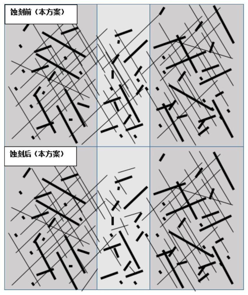
[0031] Embodiment 1: The conductive material is the conductive film of nano-silver wire + nano-silver rod + silver particles is etched

[0032] Combining conductive materials (nano-silver wire, nano-silver rod and silver particles, the diameter of the nano-silver wire is 27-30nm, the length is 5-16μm, the diameter of the silver rod is 50-200nm, the length is 0.5-10μm, the silver particle is The diameter is 50nm-5μm, wherein the content of silver nanowires is 70%, the total content of silver rods and silver particles is 30%), and the nano-silver ink with a content of 0.14wt% is coated on the surface of the substrate PET, and placed at 100 ° C for drying , after drying, apply a protective layer (OC for short) on its surface, dry at 100°C and then cure at 175°C for 5 minutes to obtain a conductive film; print the etching paste on the conductive film with a printing width of 150 μm, at 120°C Leave it for 30 minutes, and clean it with water after etching.

[0033] The schematic di...

Embodiment 2

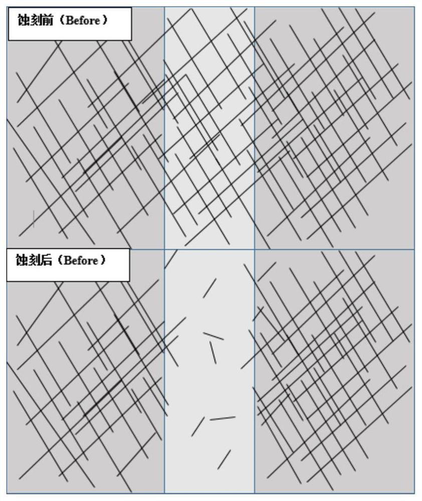
[0034] Embodiment 2: Etching the conductive film whose conductive material is nano-silver wire+gold-coated silver nano-wire

[0035] Combining conductive materials (nanometer silver wire and gold-coated silver nanowire, the diameter of the nano-silver wire is 27-30nm, the length is 5-16μm, the diameter of the gold-coated silver nanowire is 30-50nm, the length is 5-16μm, and the nano-silver The content of wire is 80%) and the nano-silver ink with 0.14wt% content is coated on the surface of the substrate PET, placed at 100 ° C for drying, after drying, the surface is coated with a protective layer (OC for short), after drying at 100 ° C Place at 175° C. for 5 minutes to cure to obtain a conductive film; print the etching paste on the conductive film with a printing width of 150 μm, place it at 120° C. for 30 minutes, and clean it with water after etching.

[0036] The silver wires in the etching area are etched, but the gold-coated silver nanowires are almost not etched, and the...


PUM

PropertyMeasurementUnit
lengthaaaaaaaaaa
diameteraaaaaaaaaa
diameteraaaaaaaaaa

Abstract

The invention discloses a method for reducing etching marks of a silver nanowire conductive film, which mainly comprises the following steps of: (1) preparing conductive material ink which is composed of fine silver nanowires and metal elementary substances or compounds difficult to etch; (2) coating the surface of the substrate with the conductive material ink to form a conductive layer; (3) coating the surface of the conductive layer with a protection layer to prepare a silver nanowire conductive film; and (4) etching the silver nanowire conductive film according to a preset pattern. As a silver nanowire in the conductive material is easy to etch, and other metal elementary substances or compounds (such as metal nanorods, metal nanoparticles, metal nanosheets and passivated or metal-coated nanomaterials) are not completely etched due to relatively large sizes or low surface activity, optical supplement to an etching region is realized, and etching marks are further reduced. Compared with traditional cut-off etching of silver wires of the same specification, the method provided by the invention is large in process regulation and control space, can superpose effects, and is suitable for large-size conductive films.

Description

technical field [0001] The invention relates to the field of conductive touch materials, in particular to a method for reducing etching marks of nano-silver wire conductive films. Background technique [0002] As one of the hottest new touch materials in recent years, nano-silver wire has the advantages of good conductivity, strong bending resistance, high transmittance, and mature mass production technology. It is currently the most likely to replace ITO as a conductive touch nanotechnology to control materials. Nano-silver conductive film, like ITO, plays the role of transmitting signals. It needs to be spread on the surface of the substrate to form a conductive layer, and then form channels by laser or etching paste yellow photoetching for signal and position information. transmission. However, due to the scattering and reflection of light by silver, when the silver nanowires are etched, there is a large difference in the scattering and reflection of light between the e...

Claims


Application Information

Patent Timeline
Patent Type & Authority Applications(China)
IPC IPC(8): H01B13/00
CPCH01B13/00
Inventor 殷志豪徐林彭颖杰
Owner NUOVO FILM SUZHOU CHINA INC
Why Eureka
Try Eureka