Method for manufacturing semiconductor laser diode and semiconductor laser diode

A technology of laser diode and manufacturing method, which is applied to the structural details of semiconductor lasers, the structure of semiconductor lasers, and optical waveguide semiconductors, etc., can solve the problems of light absorption on the end face of resonators and the like

Pending Publication Date: 2021-10-12
ASAHI KASEI KK
View PDF5 Cites 1 Cited by
  • Summary
  • Abstract
  • Description
  • Claims
  • Application Information

AI Technical Summary

Problems solved by technology

[0005] In Patent Document 1, it is described that the end face of the resonator formed by dry etching is damaged by ions and is in a state where defects are generated, so there is a problem that light absorption occurs at the end face of the resonator.

Method used


Image

  • Method for manufacturing semiconductor laser diode and semiconductor laser diode
  • Method for manufacturing semiconductor laser diode and semiconductor laser diode
  • Method for manufacturing semiconductor laser diode and semiconductor laser diode

Examples


Embodiment Construction

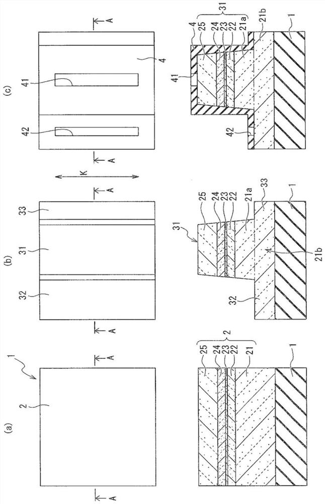
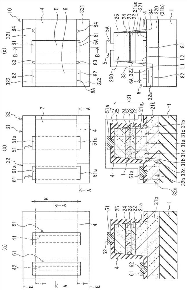
[0041]Obtained the following insight: when the resonator end face is formed by using the etching technique, the resonator end face and the end face in the resonance direction of the resonance region of the second electrode are not in the same plane, and the resonator end face exists in a plane that is lower than that of the electrode when viewed from above. This is one of the reasons for increasing the threshold current density.

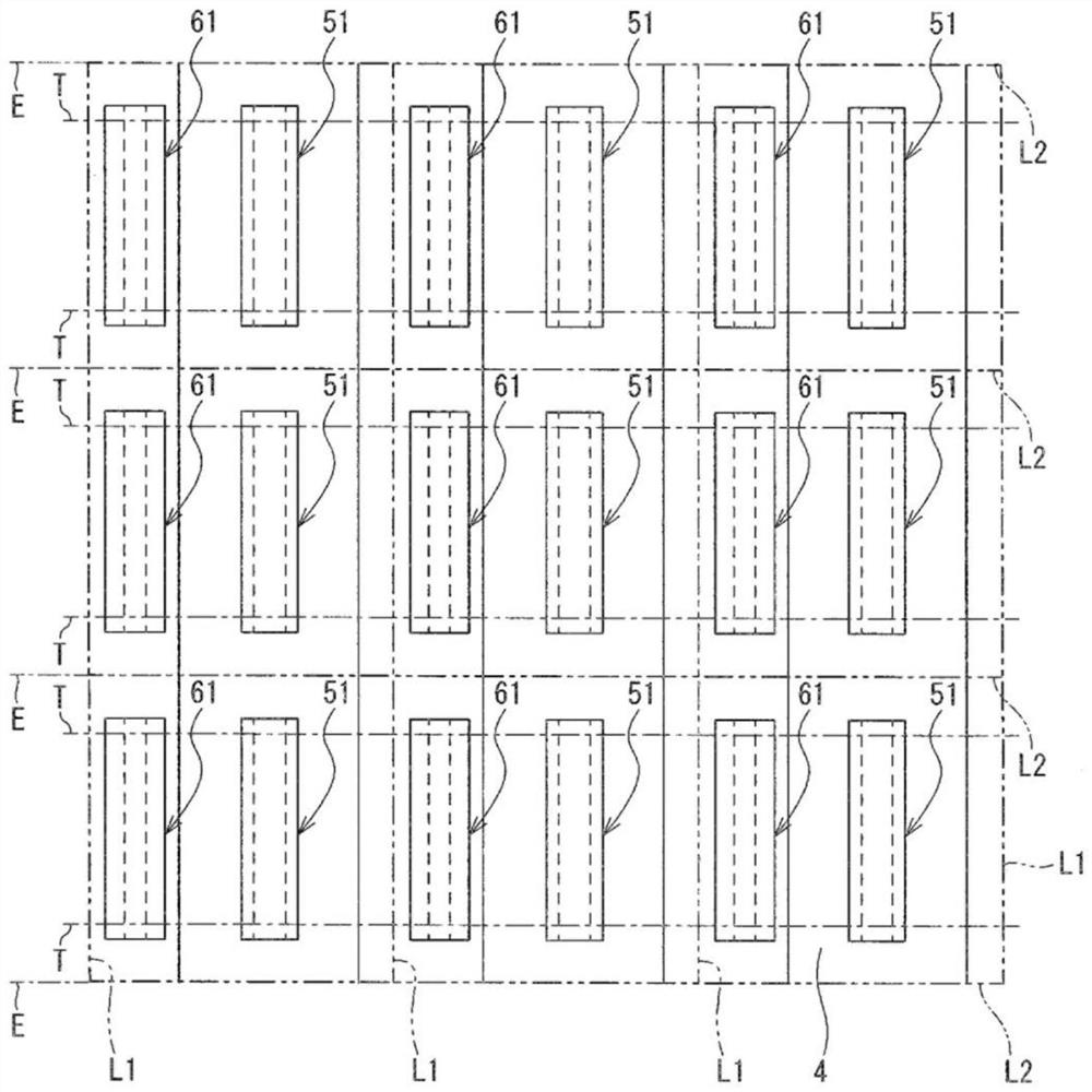
[0042] In addition, it was found that: before the process of dividing, if the inspection of the characteristics of each semiconductor laser diode is performed by contacting the terminal connected to the external power supply with the second electrode and the first electrode, the defective wafer can be removed and the reduction can be reduced. manufacturing cost.

[0043] [implementation mode]

[0044] Embodiments of the present invention will be described below, but the present invention is not limited to the embodiments shown below. In the embodim...


PUM

PropertyMeasurementUnit
thicknessaaaaaaaaaa
thicknessaaaaaaaaaa
thicknessaaaaaaaaaa

Abstract

A diode in which the threshold current density for laser oscillation is reduced is provided as a Fabry-Perot semiconductor laser diode obtained through a step of forming a resonator end face using an etching technology. A method for manufacturing a semiconductor laser diode includes a step of forming a plurality of semiconductor laser diodes on a substrate, and then dividing the substrate into each semiconductor laser diode. The method includes a step of forming a laminate on the substrate; a step of etching the laminate to separate the laminate into a portion serving as a resonance region and the other portion; an electrode layer forming step of forming a layer forming the second electrode on the second semiconductor layer of the laminate between positions where a resonator end face is formed in the resonance region and divided; after the electrode layer forming step, an etching step of simultaneously or sequentially performing the removal of a portion formed at a position on the outer side relative to the resonator end face of the layer serving as the second electrode and the formation the resonator end face.

Description

technical field [0001] The invention relates to a method for manufacturing a semiconductor laser diode. Background technique [0002] There are various types of semiconductor laser diodes depending on the structure, and one of them is a Fabry-Perot type semiconductor laser diode that resonates and amplifies light generated in a resonance region between resonator facets. [0003] As methods for forming the facets of the resonator, there are a method of cutting along the cleavage plane of the crystal and a method of using an etching technique. The method using the etching technique can be applied even when the cleavage planes of the substrate and the nitride semiconductor on the substrate are different, and has high versatility, so it is generally put into practical use. [0004] Patent Document 1 and Patent Document 2 describe methods of forming end faces of resonators using an etching technique. [0005] In Patent Document 1, it is described that the facets of resonators f...

Claims


Application Information

Patent Timeline
Patent Type & Authority Applications(China)
IPC IPC(8): H01S5/02H01S5/028H01S5/042
CPCH01S5/028H01S5/0201H01S5/0425H01S5/0203H01S5/0287H01S5/04254H01S2301/176H01S5/22H01S5/0213H01S5/04257H01S5/2086H01S5/1082H01S5/32341H01S5/04252H01S5/320225H01S5/34333H01S5/2275H01S5/4025
Inventor 佐藤恒辅岩谷素显
Owner ASAHI KASEI KK
Why Eureka
Try Eureka