
Anti-short-circuit high-voltage circuit board and manufacturing method thereof

A manufacturing method and high-voltage technology, applied in the field of PCB manufacturing, can solve the problems of reduced wiring density, increased cost, and increased product volume, and achieved the effect of preventing internal short circuits and improving withstand voltage capability.

Pending Publication Date: 2021-10-15
KUSN HULI MICROELECTRONICS
View PDF4 Cites 0 Cited by
  • Summary
  • Abstract
  • Description
  • Claims
  • Application Information

AI Technical Summary

Problems solved by technology

These two methods mean that the wiring density of the PCB will be reduced, the product volume will be increased, and the cost will be increased, thereby reducing the competitiveness of the product.

Method used


Image

  • Anti-short-circuit high-voltage circuit board and manufacturing method thereof
  • Anti-short-circuit high-voltage circuit board and manufacturing method thereof
  • Anti-short-circuit high-voltage circuit board and manufacturing method thereof

Examples


Embodiment 1

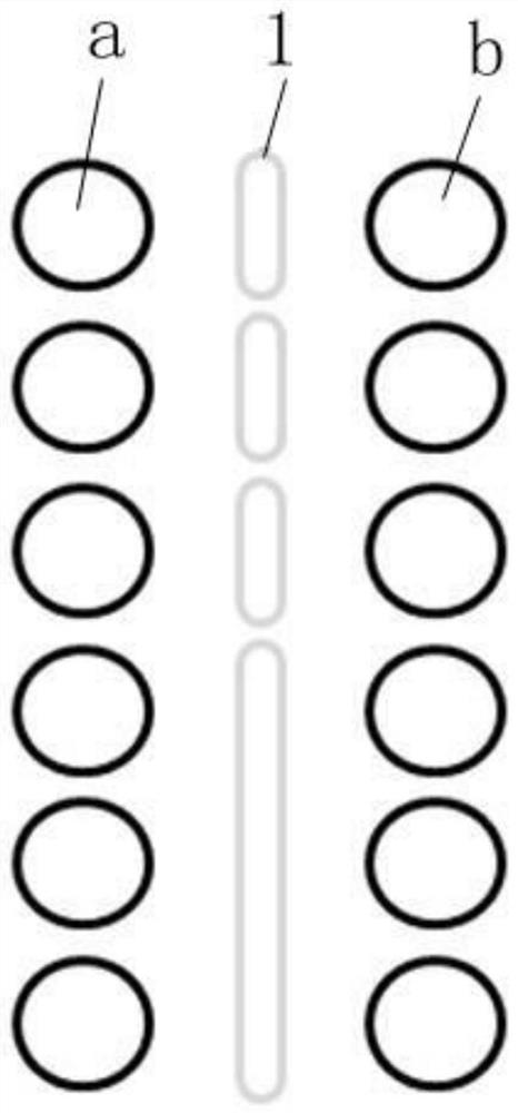
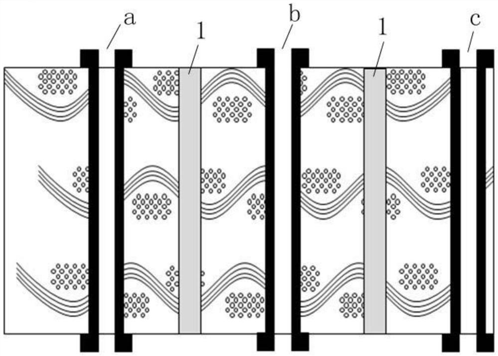
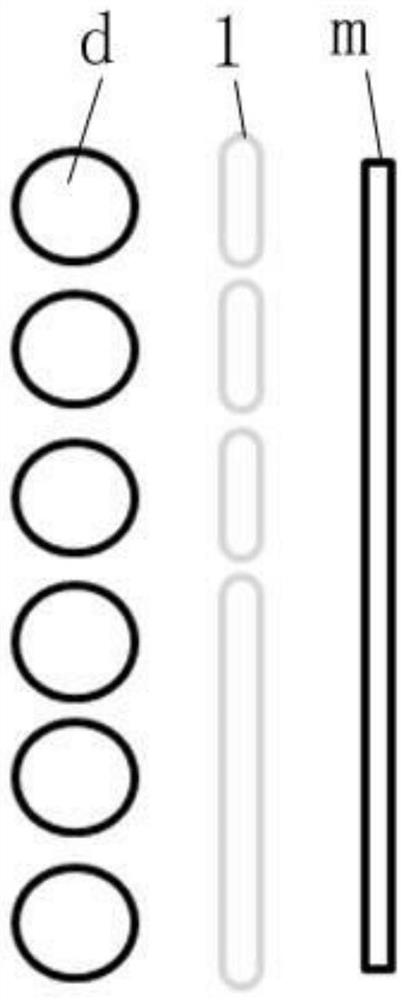
[0025] A method for manufacturing a short-circuit-proof high-voltage circuit board, comprising: between through holes with voltage differences on the high-voltage circuit board ( figure 1 Between the through hole a and the through hole b; figure 2 between through hole a and through hole b, through hole b and through hole c), between the through hole and the line where there is a voltage difference ( image 3 Between the through hole d and the line m; Figure 4 Make isolation holes between through hole d and line m, through hole e and line n, line m and through hole e).

[0026] In this embodiment, the isolation hole is a slotted hole 1 with a non-conductive inner wall processed by milling; the length of the slotted hole 1 is equal to or greater than the diameter of the corresponding through hole; The projected area on the through hole or line with which there is a voltage difference is completely shielded. The base material of high-voltage circuit boards contains glass fib...

Embodiment 2

[0028] The difference between this embodiment and Embodiment 1 is that the isolation hole is one drilled or several continuous non-perforated holes, and the continuous several non-perforated holes are tangent or intersected to form a string of non-perforated holes. The diameter of the non-through hole is equal to or greater than the diameter of the corresponding through hole. If the non-through hole string is used, the length of the non-through hole string is equal to or greater than the diameter of the corresponding through hole; and the setting position satisfies: the corresponding through hole is placed on another The projected area on a through hole or line with which there is a voltage difference is completely shielded. Such as Figure 5~Figure 8 shown in Figure 5 Among them, the length of the uppermost non-through hole 2 is longer than the diameter of the corresponding topmost through hole A and through hole B, and the non-through hole 2 completely covers the projectio...

Embodiment 3

[0030] Based on the manufacturing method of the short-circuit-proof high-voltage circuit board described in Embodiment 1 and Embodiment 2, this embodiment provides a short-circuit-proof high-voltage circuit board. There is an isolation hole between the through hole and the line where there is a voltage difference. The isolation hole is a non-conductive slot on the inner wall. The length of the slot is equal to or greater than the diameter of the corresponding through hole; The projected area of ​​is completely covered. Or the isolation hole is one or several consecutive non-perforated holes, and the continuous several non-perforated holes are tangent or intersected to form a series of non-perforated holes; the diameter of the non-perforated holes is equal to or greater than the diameter of the corresponding through-holes. The non-through hole string, the length of the non-through hole string is equal to or greater than the diameter of the corresponding through hole; and the s...


PUM


Abstract

The invention discloses an anti-short-circuit high-voltage circuit board and a manufacturing method thereof in the technical field of PCB manufacturing. The manufacturing method comprises the following steps: manufacturing isolation holes between through holes with voltage difference and between through holes with voltage difference and a circuit on the high-voltage circuit board; and on the premise that the distance between the conductors is not increased and special insulating materials are not selected, a path for forming electrochemical migration between the conductors is cut off by a physical method, and the voltage resistance between the conductors is improved.

Description

technical field [0001] The invention belongs to the technical field of PCB manufacturing, and in particular relates to a short-circuit-proof high-voltage circuit board and a manufacturing method thereof. Background technique [0002] Printed circuit board, abbreviated as PCB, is the basis of modern electronic products, and generally has one or more conductor layers, which play the role of installing and connecting components. PCBs generally use glass fiber cloth coated with insulating resin as a carrier and insulating material. The surface of the glass fiber cloth is generally coated with a layer of silane as a coupling agent to form a relatively stable coupling with the insulating resin. On double-layer and multi-layer PCBs, through-holes are generally processed by mechanical drilling, and most of them will be copper-plated on their side walls, generally called through-holes, which serve to connect various conductor layers or serve as part of components. Or the role of th...

Claims


Application Information

Patent Timeline
Patent Type & Authority Applications(China)
IPC IPC(8): H05K3/40H05K1/11
CPCH05K3/4038H05K1/115
Inventor 凌朔托德.拉塞尔.约翰逊高晨
Owner KUSN HULI MICROELECTRONICS
Learn More