Clean room system for semiconductor manufacturing and multistage electric field dust removal method thereof

An electric field dust removal and clean room technology, applied in the field of air purification, can solve the problems of electrostatic dust removal efficiency and excessive ozone concentration, high power consumption of air purification technology, and inability to remove air, etc., and achieves low cost, small size, and power consumption. saving effect

Pending Publication Date: 2021-10-22
SHANGHAI BIXIUFU ENTERPRISE MANAGEMENT CO LTD
View PDF0 Cites 0 Cited by
  • Summary
  • Abstract
  • Description
  • Claims
  • Application Information

AI Technical Summary

Problems solved by technology

[0008] In view of the shortcomings of the prior art described above, the purpose of the present invention is to provide a clean room system for semiconductor manufacturing and its multi-stage electric field dust removal method, to solve the contradiction between electrostatic dust removal efficiency and excessive ozone concentration, and the existing semiconductor manufacturing At least one technical problem of air purification technology in the field of large power consumption, large volume, high cost, and inability to remove nano-scale particles in the air

Method used


Image

  • Clean room system for semiconductor manufacturing and multistage electric field dust removal method thereof
  • Clean room system for semiconductor manufacturing and multistage electric field dust removal method thereof
  • Clean room system for semiconductor manufacturing and multistage electric field dust removal method thereof

Examples


Embodiment 1

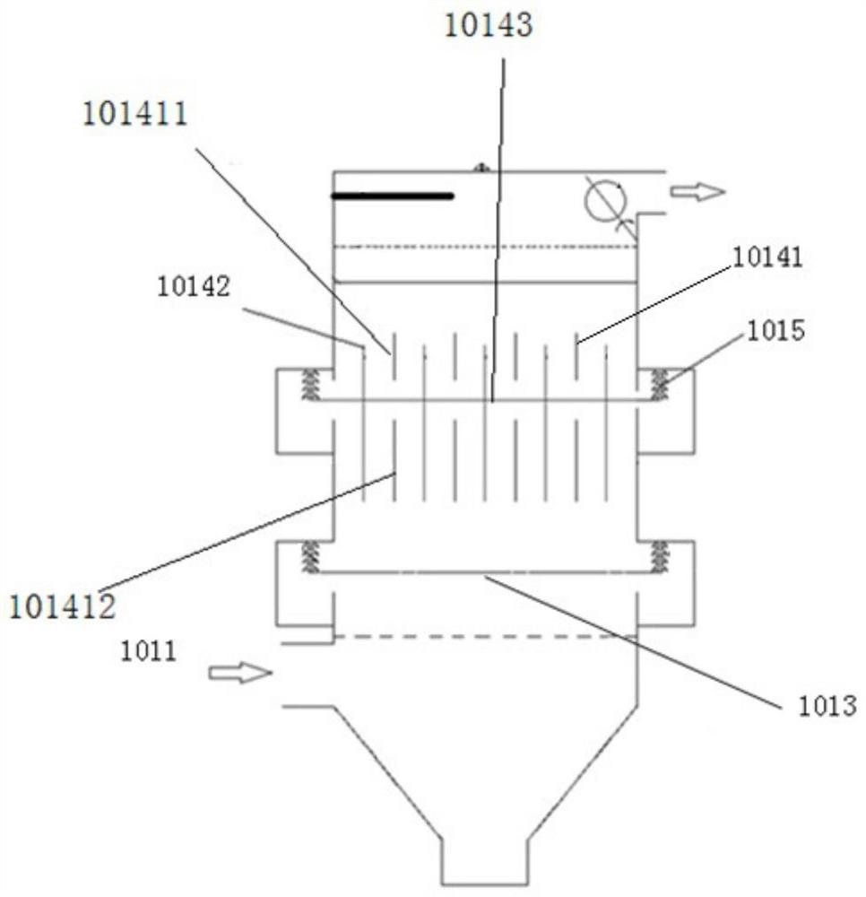
[0271] see figure 1 , which is a schematic structural diagram of the first-stage electric field device in the multi-stage electric field dust removal system of this embodiment. The electric field device includes an electric field device inlet 1011 , a front electrode 1013 , and an insulating mechanism 1015 .

[0272] The front electrode 1013 is arranged at the entrance 1011 of the electric field device. The front electrode 1013 is a conductive mesh plate, and the conductive mesh plate is used to conduct electrons to the gas with strong conductivity after power on. pollutants such as metal dust, mist droplets, or aerosols, the anode dust accumulation part of the electric field device, that is, the electric field anode 10141, attracts charged pollutants, and makes the charged pollutants move to the electric field anode until this part of the pollutants Attached to the electric field anode, this part of the pollutants are collected.

[0273] The electric field device includes a...

Embodiment 2

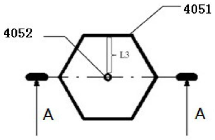
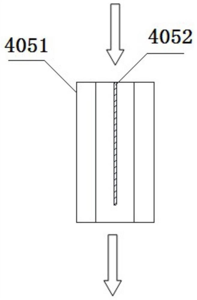
[0280] The electric field generating unit in this embodiment can be applied to the first-stage electric field device in the multi-stage electric field dust removal system of the semiconductor manufacturing clean room system of the present invention. The structure diagram of the electric field generating unit in this embodiment can be found in figure 2 , the A-A view of the electric field generating unit in this embodiment can be found in image 3 , the A-A view of the electric field generating unit of the electric field generating unit of the present embodiment marking length and angle is referred to Figure 4 .

[0281] Such as figure 2 As shown, it includes an electric field anode 4051 and an electric field cathode 4052 for generating an electric field, and the electric field anode 4051 and the electric field cathode 4052 are respectively electrically connected to two electrodes of a power supply, and the power supply is a DC power supply, and the electric field anode 405...

Embodiment 3

[0289] In this embodiment, the electric field generating unit can be applied to the first-stage electric field device in the multi-stage electric field dust removal system of the semiconductor manufacturing clean room system of the present invention, such as figure 2 As shown, it includes an electric field anode 4051 and an electric field cathode 4052 for generating an electric field, and the electric field anode 4051 and the electric field cathode 4052 are respectively electrically connected to two electrodes of a power supply, and the power supply is a DC power supply, and the electric field anode 4051 and the electric field cathode 4052 The electric field cathode 4052 is electrically connected to the anode and cathode of the DC power supply respectively. In this embodiment, the electric field anode 4051 has a positive potential, and the electric field cathode 4052 has a negative potential.

[0290] In this embodiment, the direct current power supply may specifically be a d...


PUM

PropertyMeasurementUnit
diameteraaaaaaaaaa
diameteraaaaaaaaaa
lengthaaaaaaaaaa

Abstract

The invention provides a clean room system for semiconductor manufacturing and a multi-stage electric field dust removal method thereof. The clean room system comprises a clean room and a multi-stage electric field dust removal system; the multi-stage electric field dust removal system comprises at least two electric field devices connected in series and further comprises a power supply, and an electric field anode and an electric field cathode of each electric field device are electrically connected with two electrodes of the power supply device respectively; the voltage value of the power supply of the electric field device is enough to ensure that the total dust removal efficiency (100%-(100%-P1%) * (100%-P2%) *...... * (100%-Pn%) of the electric field dust removal system is greater than a preset value, the ozone output quantity is smaller than a preset value, P1%, P2%...... Pn% are the dust removal efficiency of the first-stage electric field device, the dust removal efficiency of the second-stage electric field device,..., the dust removal efficiency of the n-th-stage electric field device respectively in sequence, and n is an integer greater than 1.

Description

technical field [0001] The invention belongs to the field of air purification, in particular to a clean room system for semiconductor manufacturing and a multistage electric field dust removal method thereof. Background technique [0002] With the advancement of technology, the size of semiconductor devices is getting smaller and smaller, and the requirements for the environment of semiconductor manufacturing workshops are also getting higher and higher. The clean room is a commonly used manufacturing workshop environment in the semiconductor manufacturing process. The purpose is to prevent particles, humidity, temperature, etc. from polluting semiconductor materials, thereby affecting the yield and reliability of semiconductors. According to the cleanliness requirements of the production process for the production environment, each clean room has different air cleanliness levels, which are usually divided by the maximum concentration limit of a certain particle size in the ...

Claims


Application Information

Patent Timeline
Patent Type & Authority Applications(China)
IPC IPC(8): B03C3/04B03C3/34B03C3/41B03C3/45B03C3/66B03C3/70
CPCB03C3/04B03C3/34B03C3/41B03C3/45B03C3/66B03C3/70
Inventor 唐万福赵晓云王大祥段志军邹永安奚勇
Owner SHANGHAI BIXIUFU ENTERPRISE MANAGEMENT CO LTD
Why Eureka
Try Eureka