Light emitting diode

A technology of light-emitting diodes and negative poles, which is applied in the direction of electrical components, circuits, semiconductor devices, etc., can solve the problems of light-emitting diode reliability and shortened life, device failure, rework temperature and tin amount can not be accurately controlled, etc., to improve resistance to high temperature deformation Capability and sealing performance, reduction of product cost and quality cost, and effect of solving the problem of resin cracking

Inactive Publication Date: 2021-10-22
GREE ELECTRICHEFEI +1
View PDF4 Cites 0 Cited by
  • Summary
  • Abstract
  • Description
  • Claims
  • Application Information

AI Technical Summary

Problems solved by technology

[0003] There is a gap between the epoxy resin and the copper substrate of the light-emitting diode currently used, and the sealing performance is poor. Due to the large difference in thermal expansion coefficient of the two materials, the resin is deformed under high temperature during welding, and the gap is further increased.
If the amount of printed tin is too much, the tin will climb up to the joint between the copper substrate and the resin and penetrate into the interior along the gap and the copper substrate. Due to the effect of tin stress on the resin, the cracks will be further aggravated. If the resin cracks reach a certain level beyond the retention of the solder joints The second bonding solder joint will have problems such as desoldering and gold wire disconnection, which will lead to device failure. Even if the diode returns to normal after cooling, it may not fail immediately, but there are still unstable factors. The reliability and life of the light emitting diode are large. In addition, the rework failure rate of SMD diodes is very high, and the rework temperature and tin amount cannot be accurately controlled, which seriously affects the reliability of light-emitting diodes.

Method used


Image

  • Light emitting diode
  • Light emitting diode
  • Light emitting diode

Examples


Embodiment Construction

[0037] The present invention will be further described in detail below in conjunction with the accompanying drawings and specific embodiments, but the protection scope of the present invention is not limited thereby.

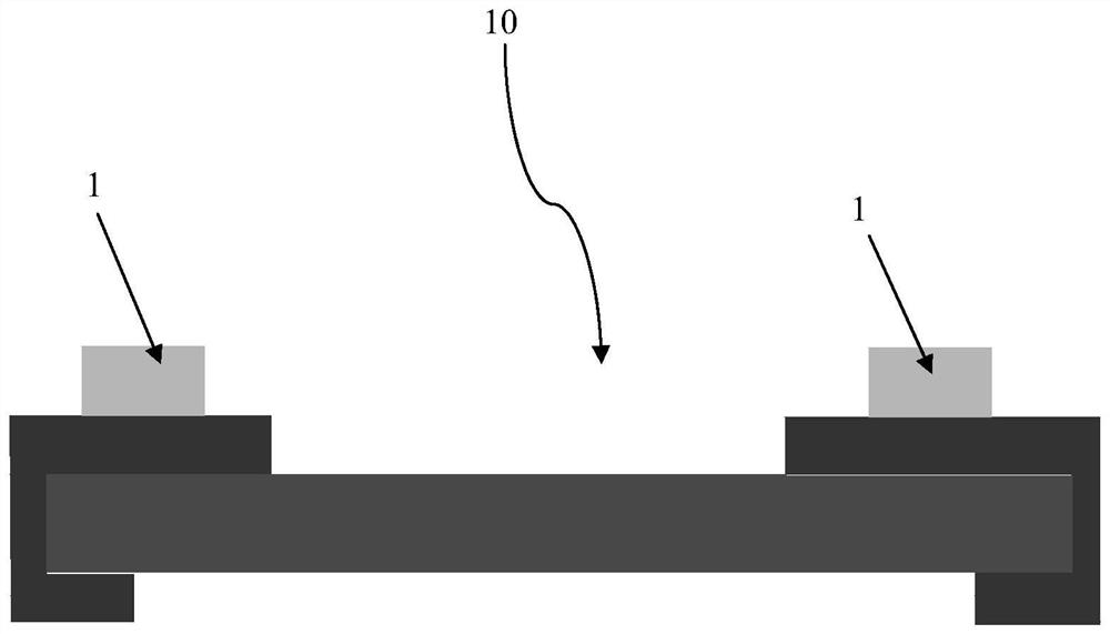
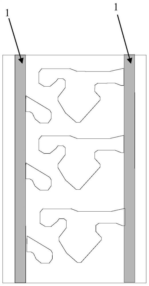
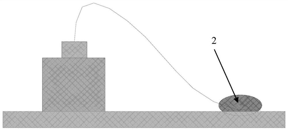
[0038] figure 1 The overall structure of the light emitting diode 10 according to the embodiment of the present invention is schematically shown. figure 2 A printing template of a light emitting diode 10 according to an embodiment of the present invention is schematically shown. image 3 It schematically shows the welding structure of the gold wire in the embodiment of the present invention. Figure 4 It schematically shows the top view structure of the gold wire welding structure in the embodiment of the present invention. Figure 5 It schematically shows the front view structure of the gold wire welding structure in the embodiment of the present invention. Image 6 The overall structure of the light emitting diode 10 according to the embodiment of the pres...


PUM

PropertyMeasurementUnit
widthaaaaaaaaaa

Abstract

The invention provides a light-emitting diode. Solder mask layers are arranged on a positive electrode area and a negative electrode area on a bonding pad of the light-emitting diode. According to the light-emitting diode provided by the invention, the production process is adjusted, and the solder mask layer is added to avoid the failure caused by solder paste permeation in the welding process. For the problems of sealing-off of the second welding spot and the like, the reliability of the welding spot is improved by adding gold balls, reinforcing silver paste and the like; therefore, the structure improves the reliability of the light-emitting diode, does not affect the use effect, and is high in practicability.

Description

technical field [0001] The invention relates to the technical field of light emitting diode structure design, in particular to a light emitting diode. Background technique [0002] Light-emitting diodes have been used as a general-purpose electronic component in all aspects of life, including daily lighting, electrical display, and traffic lights. However, with the development of science and technology, new products with small size and light weight chip structure have become the mainstream trend, so chip light emitting diodes will become the most widely used electronic components in life and production. [0003] There is a gap between the epoxy resin and the copper substrate of the light-emitting diode currently used, and the sealing performance is poor. Due to the large difference in thermal expansion coefficient of the two materials, the resin is deformed under high temperature during welding, and the gap is further increased. If the amount of printed tin is too much, the...

Claims


Application Information

Patent Timeline
Patent Type & Authority Applications(China)
IPC IPC(8): H01L33/62H01L33/56
CPCH01L33/62H01L33/56
Inventor 项永金李帅王少辉陈明轩戴银燕
Owner GREE ELECTRICHEFEI
Why Eureka
Try Eureka