Vapor phase growth device and carrier used in same

A gas phase and carrier technology, which is applied in the field of carriers, can solve the problems of being unable to suppress the sharp change of the film thickness of the epitaxial film formed on the single crystal silicon wafer, and the difficulty of flattening the peripheral edge, so as to suppress the unevenness of the film thickness, The effect of uniform film thickness

Pending Publication Date: 2021-10-22
SUMCO CORP
View PDF5 Cites 0 Cited by
  • Summary
  • Abstract
  • Description
  • Claims
  • Application Information

AI Technical Summary

Problems solved by technology

[0006] However, in the ring-shaped carrier of the above-mentioned prior art, the sharp change in the film thickness of the epitaxial film formed on the peripheral edge of the single crystal silicon wafer cannot be suppressed, so there is a problem that it is particularly difficult to planarize the peripheral edge.

Method used


Image

  • Vapor phase growth device and carrier used in same
  • Vapor phase growth device and carrier used in same
  • Vapor phase growth device and carrier used in same

Examples


Embodiment Construction

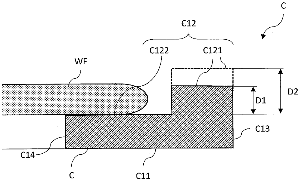
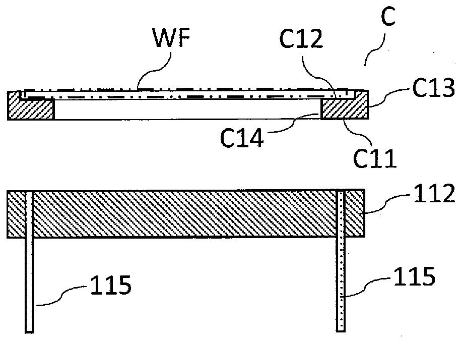
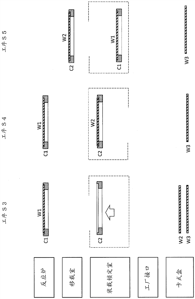
[0049] Embodiments of the present invention will be described below based on the drawings. figure 1It is a block diagram showing the vapor phase growth apparatus 1 according to the embodiment of the present invention, and the main body of the vapor phase growth apparatus 1 shown in the center is shown in plan view. The vapor phase growth apparatus 1 of this embodiment is a so-called CVD apparatus, and includes a pair of reaction furnaces 11, 11, a wafer transfer chamber 12 provided with a first robot 121 for processing a wafer WF such as a silicon single crystal wafer, and a The load lock chamber 13, the factory interface 14 provided with the second robot 141 processing the wafer WF, and the load port of the wafer storage container 15 (cassette) storing a plurality of wafers WF are provided.

[0050] The factory interface 14 is an area having the same atmosphere as that of the clean room where the wafer container 15 is placed. The factory interface 14 is provided with a secon...


PUM


Abstract

Provided is a vapor phase growth device by which the thickness of a CVD film on the edge of a wafer can be made uniform. A carrier (C) is formed into an endless ring shape and includes: a bottom surface (C11) mounted on the top surface of a susceptor (112); a top surface (C12) that contacts the outer edge of the rear surface of a wafer (WF) and supports same; an outer circumferential wall surface (C13); and an inner circumferential wall surface (C14). The structure or shape of the top surface (C12) in the circumferential direction is a structure or shape having a correspondence relationship with respect to the crystal orientation in the circumferential direction of the wafer (WF). A wafer that has yet to be processed is mounted on the carrier such that the crystal orientation in the circumferential direction of the wafer that has yet to be processed and the structure or shape of the wafer in the circumferential direction have a correspondence relationship.

Description

technical field [0001] The present invention relates to a vapor phase growth apparatus used in the manufacture of epitaxial wafers, etc., and a carrier used in the vapor phase growth apparatus. Background technique [0002] In a vapor phase growth apparatus used in the manufacture of epitaxial wafers, etc., in order to minimize damage to the back surface of the silicon wafer, it is proposed that the silicon wafer be mounted on a ring-shaped carrier in the state from the load lock chamber to the Transport in the process of the reaction chamber (Patent Document 1). [0003] In such a vapor phase growth apparatus, unprocessed wafers are mounted on an annular carrier waiting in the load lock chamber, while processed wafers are transported from the reaction chamber while being mounted on the annular carrier. Transfer to the load lock. [0004] Patent Document 1: US Patent Application Publication No. 2017 / 0110352. [0005] Patent Document 2: Japanese Patent Laid-Open No. 2007-2...

Claims


Application Information

Patent Timeline
Patent Type & Authority Applications(China)
IPC IPC(8): C30B35/00C30B25/12H01L21/205H01L21/673C30B29/06C23C16/44C23C16/458
CPCC30B25/12C30B29/06C30B35/005H01L21/67748H01L21/68735H01L21/67346C23C16/4585C23C16/54H01L21/205C30B35/00C23C16/44C23C16/458H01L21/673C23C16/24C23C16/4583
Inventor 和田直之南出由生
Owner SUMCO CORP
Why Eureka
Try Eureka