Ga2O3 Schottky diode based on diamond terminal structure and manufacturing method

A Schottky diode and terminal structure technology, which is applied in semiconductor/solid-state device manufacturing, electrical components, circuits, etc., can solve the problems of device performance degradation and device leakage current increase, so as to improve reliability and reduce electric field concentration , Improve the effect of reverse pressure resistance

Active Publication Date: 2021-10-26
ZHEJIANG XINKE SEMICON CO LTD
View PDF7 Cites 2 Cited by
  • Summary
  • Abstract
  • Description
  • Claims
  • Application Information

AI Technical Summary

Problems solved by technology

However, due to actual process errors, low concentration Ga 2 o 3 Ga in terminal protected area 2 o 3 The electric field concentration phenomenon in the metal edge region of the Schottky diode is still relatively obvious, resulting in increased leakage current of the device and degradation of device performance

Method used


Image

  • Ga2O3 Schottky diode based on diamond terminal structure and manufacturing method
  • Ga2O3 Schottky diode based on diamond terminal structure and manufacturing method
  • Ga2O3 Schottky diode based on diamond terminal structure and manufacturing method

Examples


Embodiment 1

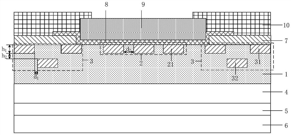
[0045] See figure 1 , figure 1 A kind of Ga based on diamond termination structure provided for the embodiment of the present invention 2 o 3 Schematic diagram of the structure of a Schottky diode. The Ga 2 o 3 Schottky diodes include: Ga 2 o 3 Epitaxial layer 1, active region 2, terminal region 3, Ga 2 o 3 A substrate 4 , an ohmic contact metal layer 5 , a first contact layer 6 , a first passivation layer 7 , a Schottky contact metal layer 8 , a second contact layer 9 and a second passivation layer 10 .

[0046] Specifically, Ga 2 o 3 The material of the epitaxial layer 1 includes N-type Ga 2 o 3 .

[0047] Active region 2 is located at Ga 2 o 3 In the surface layer of epitaxial layer 1, from Ga 2 o 3 The surface of the epitaxial layer 1 is exposed.

[0048] In a specific embodiment, the active region 2 includes several active region diamond structures 21 arranged at intervals, and the active region diamond structures 21 and Ga 2 o 3 The epitaxial layer 1 ...

Embodiment 2

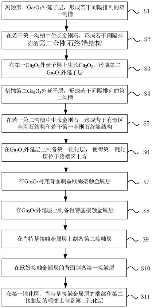
[0066] On the basis of Example 1, please refer to figure 2 and Figure 3a-Figure 3k , figure 2 A kind of Ga based on diamond termination structure provided for the embodiment of the present invention 2 o 3 Schematic flow chart of the manufacturing method of the Schottky diode, Figure 3a-Figure 3k A kind of Ga based on diamond termination structure provided for the embodiment of the present invention 2 o 3 Schematic diagram of the manufacturing method of the Schottky diode, the manufacturing method includes steps:

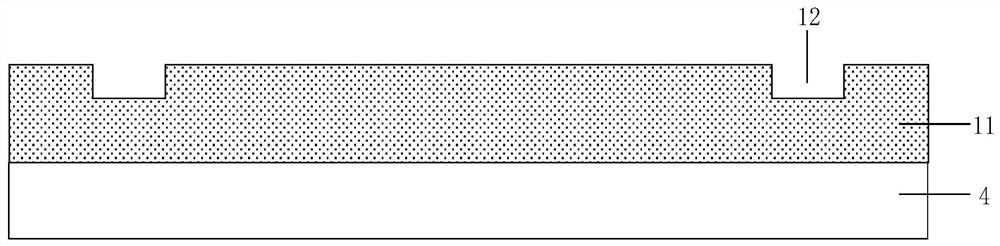
[0067] S1, etch the first Ga 2 o 3 The epitaxial sublayer 11 forms a plurality of first grooves 12 arranged at intervals, please refer to Figure 3a .

[0068] First, a sample is obtained, which includes Ga 2 o 3 Substrate 4 and the first Ga 2 o 3 Epitaxial sublayer 11, the first Ga 2 o 3 The epitaxial sublayer 11 is located in the Ga 2 o 3 on the substrate 4. First Ga 2 o 3 The material of the epitaxial sublayer 11 is N-type Ga 2 o 3 .

[00...


PUM

PropertyMeasurementUnit
thicknessaaaaaaaaaa

Abstract

The invention relates to a Ga2O3 Schottky diode based on a diamond terminal structure and a manufacturing method. The Schottky diode comprises a Ga2O3 epitaxial layer; an active region, located in the surface layer of the Ga2O3 epitaxial layer; a terminal region, located in the Ga2O3 epitaxial layer and located on the two sides of the active region. The terminal region comprises a plurality of first diamond terminal structures and a plurality of second diamond terminal structures, the first diamond terminal structures are arranged at intervals, and the second diamond terminal structures are arranged at intervals; the plurality of first diamond terminal structures and the plurality of second diamond terminal structures are alternately distributed up and down, and pn junctions are formed between the plurality of first diamond terminal structures and the Ga2O3 epitaxial layer and between the plurality of second diamond terminal structures and the Ga2O3 epitaxial layer. A surface electric field in the Schottky diode is intensively and gradually introduced into a device body, so that the phenomenon that the device is broken down in advance is avoided, the reliability of the device is improved, and the reverse voltage endurance capability of the device under normal static characteristics is improved.

Description

technical field [0001] The invention belongs to the technical field of semiconductor device structure and manufacture, in particular to a Ga 2 o 3 Schottky diode and its fabrication method. Background technique [0002] Gallium oxide (Ga 2 o 3 ) As a new type of ultra-wide bandgap semiconductor, it has a large energy band gap (about 4.9eV), high theoretical breakdown electric field (8MV / cm) and Baliga (Baliga) excellent value, these excellent properties make Gallium oxide has become a hot material for next-generation high-power electronic devices. [0003] As a basic component in semiconductor circuits, Schottky barrier diodes have great applications in radio frequency identification tags, solar cells, amplifiers, photodetectors and logic gates because of their high switching speed and low conduction loss. High-performance Schottky diodes play an important role in the field of high-voltage switching. [0004] To achieve high application reliability, Ga 2 o 3 The meta...

Claims


Application Information

Patent Timeline
Patent Type & Authority Applications(China)
IPC IPC(8): H01L29/872H01L29/06H01L21/34
CPCH01L29/872H01L29/0607H01L29/0615H01L29/0684H01L29/66969Y02P70/50
Inventor 李京波王小周赵艳齐红基
Owner ZHEJIANG XINKE SEMICON CO LTD
Why Eureka
Try Eureka