

Optical signal processing chip based on arrayed waveguide grating
An arrayed waveguide grating and processing chip technology, applied in the field of optical communication, can solve the problems of limiting performance improvement, difficult control of device size and stability, etc., to achieve the effect of reducing volume
- Summary
- Abstract
- Description
- Claims
- Application Information
AI Technical Summary
Problems solved by technology
Method used
Image


Examples
Embodiment Construction
[0026] Hereinafter, the present invention will be described in detail with reference to the accompanying drawings and examples.
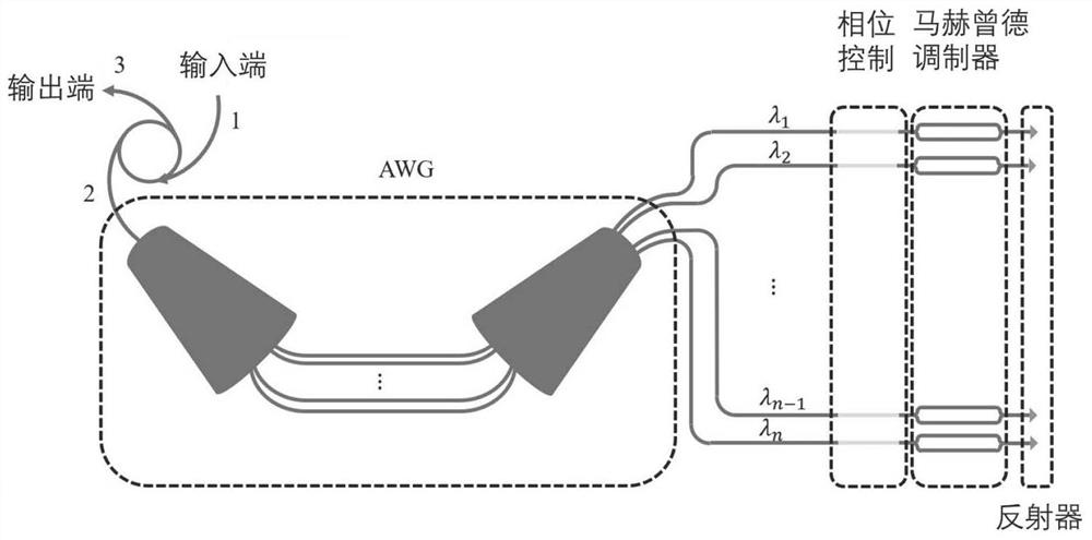
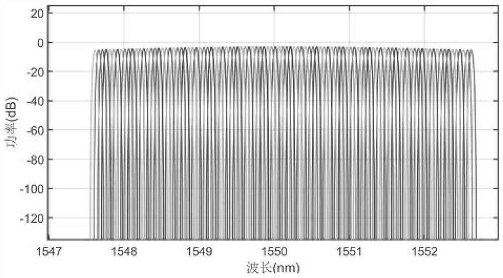
[0027] Such as figure 1 As shown, the present invention provides an optical signal processing chip based on an arrayed waveguide grating (AWG). The optical signal processing chip is based on a reflective structure and consists of an AWG, a phase and amplitude control array, and a reflector connection.
[0028] In this example, arrayed waveguide gratings, phase and amplitude control arrays, and reflectors are monolithically integrated on z-cut thin-film lithium niobate materials to achieve phase and amplitude control of different frequency components of incident light waves. Using thin-film lithium niobate material as the waveguide layer can achieve very low waveguide loss (<0.1dB / cm), thus reducing the loss of the entire optical signal processing chip. Compared with the traditional silicon-based or indium-phosphorus-based optical phased array, the ...
PUM
 Abstract
Description
Claims
Application Information