Monocrystalline silicon doping method and monocrystalline silicon manufacturing method

A single crystal silicon and dopant technology, applied in the field of solar photovoltaics, can solve the problem of uneven distribution of resistivity at the head and tail of single crystal silicon

Pending Publication Date: 2021-11-09
LONGI GREEN ENERGY TECH CO LTD
View PDF0 Cites 3 Cited by
  • Summary
  • Abstract
  • Description
  • Claims
  • Application Information

AI Technical Summary

Problems solved by technology

[0004] Embodiments of the present invention provide a single crystal silicon doping method and a single crystal silicon manufacturing method to solve the problem of uneven distribution of resistivity at the head and tail of existing single crystal silicon

Method used


Image

  • Monocrystalline silicon doping method and monocrystalline silicon manufacturing method
  • Monocrystalline silicon doping method and monocrystalline silicon manufacturing method
  • Monocrystalline silicon doping method and monocrystalline silicon manufacturing method

Examples


Embodiment 1

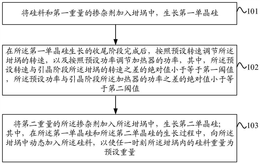
[0053] refer to figure 1 , which shows a flow chart of a single crystal silicon doping method according to an embodiment of the present invention, which may specifically include the following steps:

[0054] Step 101 , adding silicon material and a first weight of dopant into a crucible to grow a first single crystal silicon.

[0055]In the embodiment of the present invention, the silicon material may be raw polysilicon material, etc., which is not limited in the embodiment of the present invention. In order to ensure the resistivity of the single crystal silicon, the single crystal silicon needs to be doped, and the type of dopant can be determined according to the conductivity type of the target single crystal silicon. For example, when the conduction type of the target monocrystalline silicon is P-type, a trace amount of group IIIA elements, such as gallium, boron, aluminum, etc., can be doped; VA group elements, such as phosphorus, antimony, arsenic, etc. It can be unde...

Embodiment 2

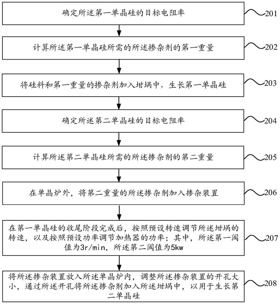
[0065] refer to image 3 , which shows a flow chart of a single crystal silicon doping method according to Embodiment 2 of the present invention, which may specifically include the following steps:

[0066] Step 201, determining the target resistivity of the first single crystal silicon.

[0067] In the embodiment of the present invention, determining the target resistivity of the first single crystal silicon includes determining the conductivity type and the value of the target resistivity of the first single crystal silicon, and the conductivity type and the target resistivity value of the single crystal silicon will directly affect the value of the single crystal silicon. The conductivity of silicon, so when monocrystalline silicon is used to make solar cells, it will affect the performance of solar cells. Its conductivity type can be P-type or N-type. The majority carriers in P-type single crystal silicon are mainly holes in single crystal silicon. The more impurities of ...

Embodiment 3

[0086] refer to Figure 4 , shows a flow chart of a single crystal silicon doping method according to Embodiment 3 of the present invention, which may specifically include the following steps:

[0087] Step 301 , adding silicon material and a first weight of dopant into a crucible to grow a first single crystal silicon.

[0088] Step 302, after the finishing stage of the growth of the first single crystal silicon is completed, the rotation speed of the crucible is adjusted according to the preset rotation speed, and the power of the heater is adjusted according to the preset power;

[0089] Step 303, adding a second weight of the dopant into the crucible to grow a second single crystal silicon.

[0090] In the embodiment of the present invention, step 301 may refer to the above-mentioned step 101, step 302 may refer to the above-mentioned step 102, and step 303 may refer to the above-mentioned step 103. To avoid repetition, details are not repeated here.

[0091] Step 304, a...


PUM

PropertyMeasurementUnit
Densityaaaaaaaaaa
Resistivityaaaaaaaaaa

Abstract

The embodiment of the invention provides a monocrystalline silicon doping method and a monocrystalline silicon manufacturing method. The monocrystalline silicon doping method comprises the steps that: a silicon material and a dopant with a first weight are added into a crucible to grow first monocrystalline silicon; after the ending stage of the growth of the first monocrystalline silicon is completed, the rotating speed of the crucible is adjusted to a preset rotating speed, and the power of a heater is adjusted to preset power, wherein the absolute value of the difference between the preset rotating speed and the rotating speed of the crucible in the seeding stage is smaller than or equal to a first threshold, and the absolute value of the difference between the preset power and the power of the heater in the seeding stage is smaller than or equal to a second threshold; and the dopant with a second weight is added into the crucible to grow second monocrystalline silicon, wherein in the growth process of the first monocrystalline silicon and the second monocrystalline silicon, the silicon material is dynamically added into the crucible, so that the weight of the silicon material in the crucible at any moment is a preset weight. The method provided by the embodiment of the invention can effectively control the amount of the dopant, improve the utilization efficiency of the dopant, and solve the problem of non-uniform resistivity distribution of the head and tail parts of monocrystalline silicon.

Description

technical field [0001] The invention relates to the field of solar photovoltaic technology, in particular to a single crystal silicon doping method and a single crystal silicon manufacturing method. Background technique [0002] Monocrystalline silicon is the most basic material for preparing solar cells. The performance of solar cells mainly depends on the quality of monocrystalline silicon, and resistivity is an important parameter reflecting the quality of monocrystalline silicon. [0003] At present, the resistivity of single crystal silicon is mainly controlled by doping a certain amount of impurities during the growth process of single crystal silicon. Since the doping of gallium element in the preparation of monocrystalline silicon can improve the overall performance of solar cells, especially the solar cells have excellent performance in terms of conversion efficiency, service life and resistance to harsh environments. Therefore, doping gallium elements is gradually ...

Claims


Application Information

Patent Timeline
IPC IPC(8): C30B15/04C30B15/20C30B29/06
CPCC30B15/04C30B15/20C30B29/06
Inventor 王建波周锐邓浩李侨付泽华张龙龙徐战军张永辉张伟建
Owner LONGI GREEN ENERGY TECH CO LTD
Why Eureka
Try Eureka