Wiring of a semiconductor switch

A circuit layout and semiconductor technology, applied in the direction of semiconductor devices, electronic switches, circuits, etc., can solve problems such as settings that cannot be optimized, and achieve the effect of a compact structure

Pending Publication Date: 2021-11-12
SIEMENS AG
View PDF0 Cites 0 Cited by
  • Summary
  • Abstract
  • Description
  • Claims
  • Application Information

AI Technical Summary

Problems solved by technology

Optimal settings cannot be achieved in this case

Method used


Image

  • Wiring of a semiconductor switch
  • Wiring of a semiconductor switch
  • Wiring of a semiconductor switch

Examples


Embodiment Construction

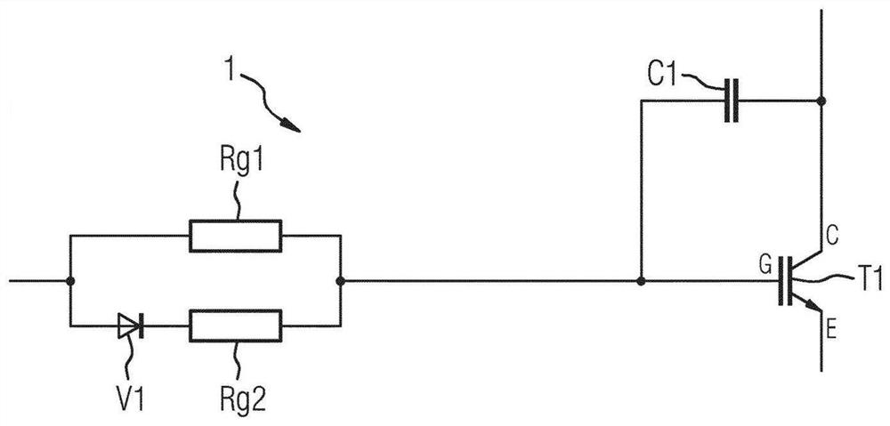
[0041] FIG. 1 shows a circuit arrangement 1 of a semiconductor switch T1 known from the prior art. The semiconductor switch T1 is, for example, a field effect transistor, in particular a MOSFET or an IGBT, and has a gate G, a collector C and an emitter E. A capacitor C1 is arranged between the collector C and the gate G. This forms a gate wiring arrangement consisting of the first gate resistor Rg1 , the second gate resistor Rg2 and the gate diode V1 , which symbolizes the gate resistors as explained above in the introduction.

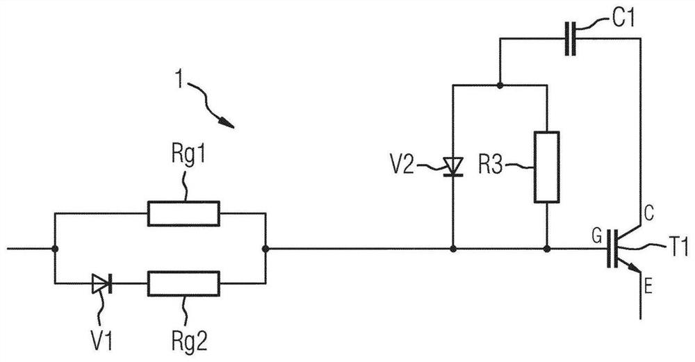
[0042] figure 2 A first embodiment of a circuit arrangement 1 of a semiconductor switch T1 is shown.

[0043] The semiconductor switch T1 is, for example, a field effect transistor, in particular a MOSFET or an IGBT, and has a gate G, a collector C and an emitter E. A capacitor C1 is arranged between the collector C and the gate G. This forms a gate wiring arrangement consisting of the first gate resistor Rg1 , the second gate resistor Rg2 and the ...


PUM


Abstract

The invention relates to a wiring (1) of a semiconductor switch (T1), the wiring comprising a gate (G), a collector (C) or a drain, and an emitter (E) or a source, wherein the wiring (1) comprises a capacitor (C1) between the gate (G) and the collector (C) or drain, and a parallel circuit of a resistor (R3) and a diode (V2) is provided in series with the capacitor (C1).

Description

technical field [0001] The invention discloses a circuit arrangement of a semiconductor switch. Background technique [0002] Voltage switching edges (du / dt) occur in the switching of semiconductors, such as IGBTs, MOSFETs, etc. This voltage switching edge extends mostly non-linearly, so that on the one hand the maximum voltage gradient (du / dt_max) and on the other hand the average voltage gradient (eg 10%-90% value) has to be considered for IGBT tuning (gate resistor tuning). [0003] For certain applications the maximum voltage gradients in the power semiconductors must be limited, since too high voltage edges cause problems with respect to electromagnetic compatibility (EMV) and in power electronic switches can lead to possible damage to machines connected to the windings. [0004] In simple control circuits, for example with only a gate resistor, the gate resistor is adapted for setting the maximum voltage gradient. If the maximum voltage gradient is limited by the ga...

Claims


Application Information

Patent Timeline
Patent Type & Authority Applications(China)
IPC IPC(8): H03K17/16H03K17/082H03K17/04H03K17/042
CPCH03K17/166H03K17/168H03K17/0828H03K17/0822H03K17/0406H03K17/04206H03K17/567H03K17/74
Inventor 露西娅·希尔施贝恩德·罗佩尔特托马斯·施温
Owner SIEMENS AG
Why Eureka
Try Eureka