Silicon carbide crystal with few small-angle grain boundaries, substrate and preparation method thereof

A silicon carbide substrate, small-angle grain boundary technology, applied in chemical instruments and methods, crystal growth, single crystal growth, etc., can solve the problems of unfavorable access to high-quality silicon carbide crystals, and achieve low stress and low dislocation density , high quality effect

Active Publication Date: 2022-07-12
SICC CO LTD
View PDF0 Cites 0 Cited by
  • Summary
  • Abstract
  • Description
  • Claims
  • Application Information

AI Technical Summary

Problems solved by technology

[0009] For the seed crystals with local defects at the edge, the defects will be inherited into the grown crystal with a high probability during the crystal growth process, so that the crystal always has the defect at the same position, which is not conducive to obtaining high-quality silicon carbide crystals

Method used


Image

  • Silicon carbide crystal with few small-angle grain boundaries, substrate and preparation method thereof
  • Silicon carbide crystal with few small-angle grain boundaries, substrate and preparation method thereof
  • Silicon carbide crystal with few small-angle grain boundaries, substrate and preparation method thereof

Examples


Embodiment 1

[0086] The diagram of this embodiment does not show the structure of the heat preservation ring, and this embodiment mainly describes the structure of the air layer.

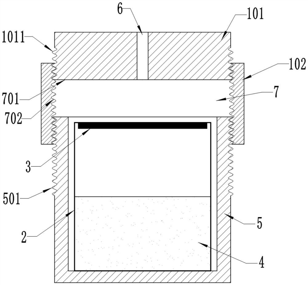
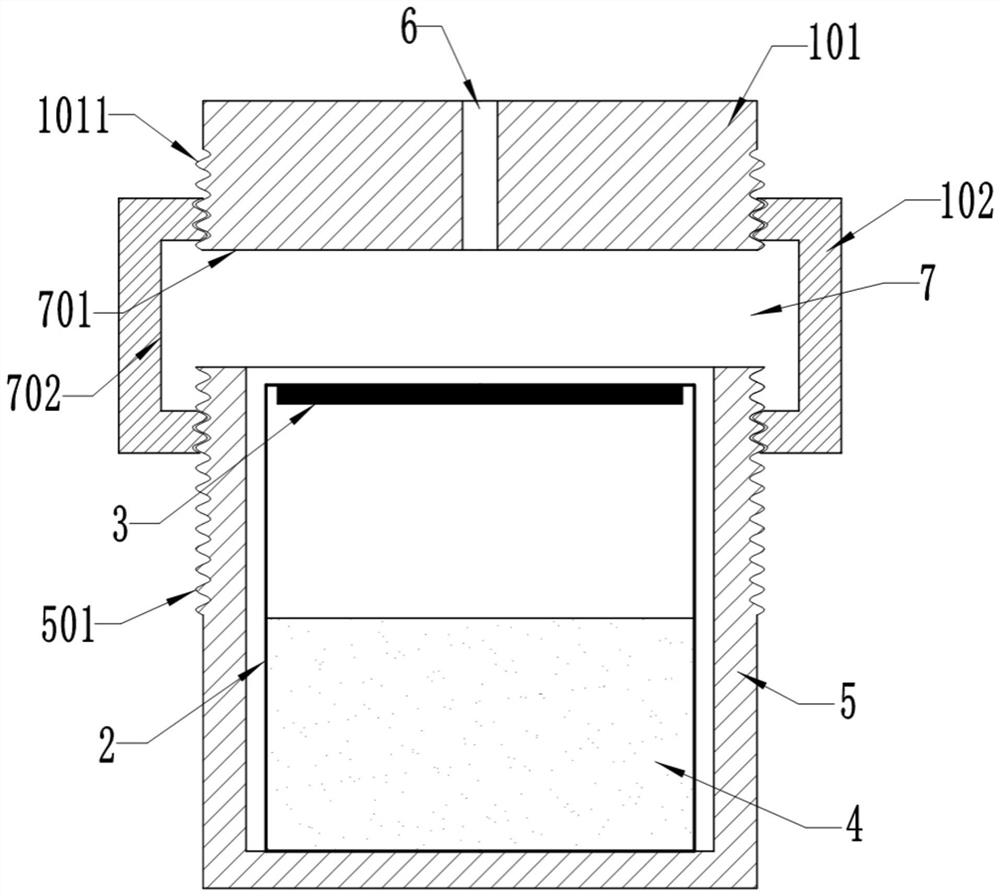
[0087] The crucible 2 is a graphite crucible, and the size of the silicon carbide seed crystal in the crucible 2 is 100-350 mm.

[0088] refer to Figure 1-3 The insulation layer includes a lower insulation layer, an upper insulation layer 101, a side insulation layer 5 and a transition insulation layer 102. The lower insulation layer, the upper insulation layer 101, the side insulation layer 5 and the transition insulation layer 102 form an insulation cavity, and the upper insulation layer 101 A temperature measuring hole is provided; the transition insulation layer 102 is at least threadedly connected to one of the upper insulation layer 101 and the side insulation layer 5, and is integrally formed with the other, and the transition insulation layer 102 is threaded between the upper insulation layer 101 and th...

Embodiment 2

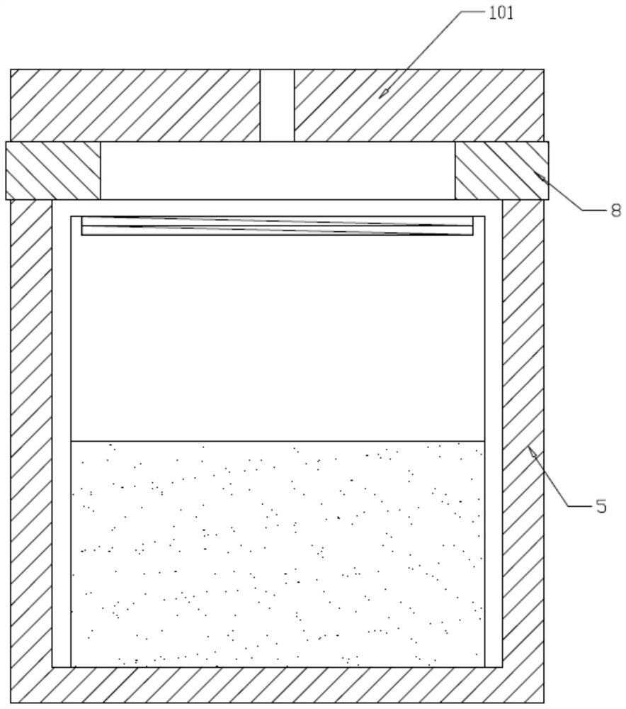
[0098] In this embodiment, a schematic diagram of the structure of adding a heat preservation ring is described in conjunction with Embodiment 1. The part not shown in Embodiment 1 in this embodiment is that a heat preservation ring can be directly placed between the crucible and the upper heat preservation layer.

[0099] refer to Figure 4 The difference between this embodiment and Example 1 is that the thermal insulation layer includes a lower thermal insulation layer, an upper thermal insulation layer 101, a side thermal insulation layer 5 and a thermal insulation ring 8, and the thermal insulation ring 8 is connected between the upper thermal insulation layer 101 and the side thermal insulation layer 5. , the lower thermal insulation layer, the upper thermal insulation layer 101, the side thermal insulation layer 5 and the thermal insulation ring 8 enclose a thermal insulation cavity.

[0100] refer to Figure 5 , this embodiment and Example 1 figure 1 The difference be...

Embodiment 3

[0104] The method for preparing a silicon carbide substrate using any of the insulating layers and the crucible contained in Embodiment 2 includes the following steps:

[0105] 1) Assembling: provide bearing raw materials and seed crystals arranged on the top of the crucible, place the crucible in the heat preservation cavity formed by the heat preservation layer, and then place it in the crystal growth furnace; wherein, the heat preservation layer includes a heat preservation ring placed above the crucible, which keeps the heat preservation effect. The ring covers at least 0.5mm to 0.5r-0.5mm extending inward from the edge of the seed crystal, where r is the radius of the seed crystal;

[0106] 2) Crystal growth: silicon carbide crystals are prepared by growing crystals, and the edges of the obtained silicon carbide crystals form an annular shape roughly corresponding to the covering position of the insulation ring;

[0107] 3) Preparing a primary silicon carbide substrate: p...


PUM

PropertyMeasurementUnit
widthaaaaaaaaaa
sizeaaaaaaaaaa
sizeaaaaaaaaaa

Abstract

The present application discloses a silicon carbide crystal with few small-angle grain boundaries, a substrate and a preparation method thereof. The silicon carbide crystal silicon carbide crystal has a ring shape, the ring shape extends from the first main surface to the second main surface, and the ring shape includes edge dislocations. The present application prepares a silicon carbide crystal with a ring shape, and applies it after mastering its related formation mechanism and testing method, so as to turn waste into treasure to optimize the edge quality of silicon carbide. The edge dislocation wall is used to prevent the edge dislocation formed in the process of SiC crystal growth from slipping inward and the edge small-angle grain boundary extending inward, and to obtain high-quality SiC substrate with the help of special processing equipment and technology.

Description

technical field [0001] The application relates to a silicon carbide crystal with few small-angle grain boundaries, a substrate and a preparation method thereof, belonging to the field of semiconductor materials. Background technique [0002] Silicon carbide has attracted widespread attention due to its excellent semi-insulating properties, especially for high-power semiconductor devices with special needs. Silicon carbide has become a potential material for these devices due to its high temperature, high frequency, and high power characteristics. . [0003] At present, the industrial production of silicon carbide crystals is mostly produced by the PVT method, but due to its high requirements for growth conditions, the defects introduced during the growth process limit its performance improvement and further application and development. Therefore, the improvement of defects has become the primary prerequisite for improving the quality of silicon carbide substrates. [0004]...

Claims


Application Information

Patent Timeline
Patent Type & Authority Patents(China)
IPC IPC(8): C30B29/36C30B23/00C30B23/02
CPCC30B29/36C30B23/025C30B23/002
Inventor 张九阳李霞王永方王宗玉张红岩高超薛刚生杜其健苏丽娜
Owner SICC CO LTD
Why Eureka
Try Eureka