
Silicon-based electro-optical modulator and preparation method thereof

An electro-optical modulator, a silicon-based technology, applied in light guides, optics, instruments, etc., can solve the problem of non-linear modulation speed and insertion loss, and achieve the effect of small insertion loss

Pending Publication Date: 2021-11-23
INST OF SEMICONDUCTORS - CHINESE ACAD OF SCI
View PDF0 Cites 0 Cited by
  • Summary
  • Abstract
  • Description
  • Claims
  • Application Information

AI Technical Summary

Problems solved by technology

The bandwidth of the silicon electro-optic modulator based on the plasmonic dispersion effect is limited by the carrier transport time, which is difficult to improve, and doping causes the modulation speed and nonlinearity to decrease and brings insertion loss

Method used


Image

  • Silicon-based electro-optical modulator and preparation method thereof
  • Silicon-based electro-optical modulator and preparation method thereof
  • Silicon-based electro-optical modulator and preparation method thereof

Examples


preparation example Construction

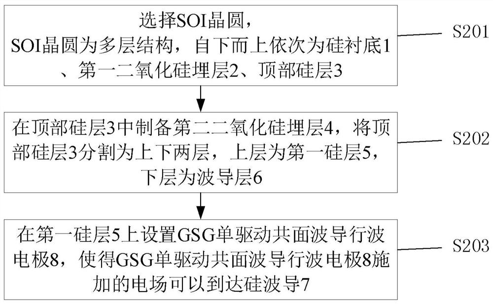
[0031] The preparation method of the silicon-based electro-optic modulator of the present invention is introduced below. like figure 2 It is a schematic flow chart of the method for preparing a silicon-based electro-optic modulator of the present invention, including:

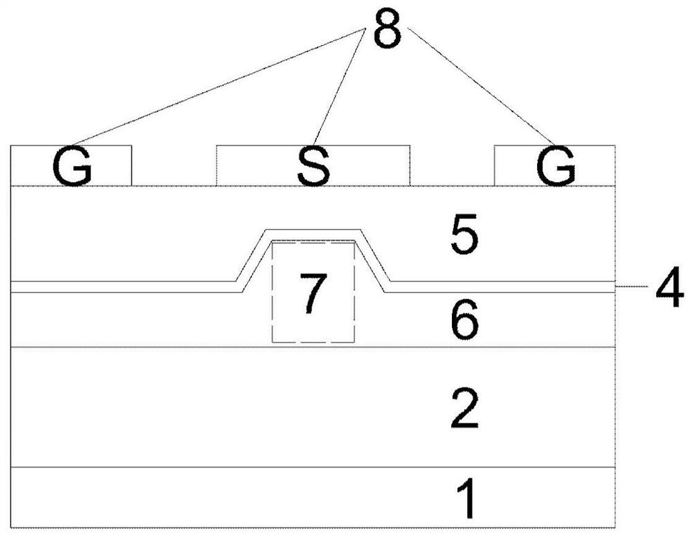
[0032] S201 , selecting an SOI wafer. The SOI wafer has a multi-layer structure, including a silicon substrate 1 , a first silicon dioxide buried layer 2 , and a top silicon layer 3 in sequence from bottom to top. The thickness of the top silicon layer 3 is preferably 600 nm.

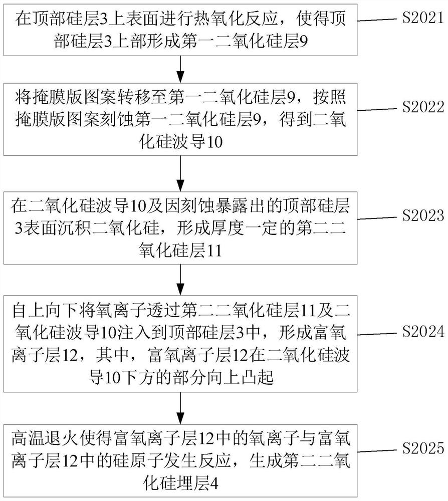
[0033] S202 , preparing a second silicon dioxide buried layer 4 in the top silicon layer 3 , and dividing the top silicon layer 3 into upper and lower layers, the upper layer being the first silicon layer 5 , and the lower layer being the waveguide layer 6 .

[0034] In step S202 , a part of the prepared second silicon dioxide buried layer 4 protrudes upwards, so that the lower waveguide layer 6 forms a ridge structure, and the upward...


PUM

PropertyMeasurementUnit
thicknessaaaaaaaaaa
thicknessaaaaaaaaaa
thicknessaaaaaaaaaa

Abstract

The invention provides a silicon-based electro-optical modulator and a preparation method thereof. The method comprises the steps: an SOI wafer is selected, and the SOI wafer is of a multi-layer structure and comprises a silicon substrate, a first silicon dioxide buried layer and a top silicon layer from bottom to top; a second silicon dioxide buried layer is prepared in the top silicon layer, the top silicon layer is divided into an upper layer and a lower layer, the upper layer is a first silicon layer, the lower layer is a waveguide layer, a part of the second silicon dioxide buried layer protrudes upwards to enable the waveguide layer below to form a ridge-shaped structure, the upward protruding part of the ridge-shaped structure is a silicon waveguide, and pressure stress exists in the second silicon dioxide buried layer; the first silicon layer and the waveguide layer are extruded outwards, so that the left upper corner and the right upper corner of the silicon waveguide are extruded to cause atom arrangement change, and second-order nonlinear polarizability is induced in the silicon waveguide; and a GSG single-drive coplanar waveguide traveling wave electrode is arranged on the first silicon layer, so that an electric field applied by the GSG single-drive coplanar waveguide traveling wave electrode can reach the silicon waveguide. The problem that the bandwidth of a conventional silicon electro-optical modulator is limited by carrier transport time and is difficult to improve is solved, insertion loss is small, and 3D photon integration can be achieved.

Description

technical field [0001] The invention relates to a silicon-based electro-optic modulator and a preparation method thereof. Background technique [0002] The silicon base has the advantages of small size, low energy consumption, CMOS process compatibility, and the convenience of monolithic and micro-nano integration with existing electronic devices and photonic devices. The silicon base is used to realize light generation, modulation, transmission, manipulation and detection, etc. Functional silicon photonics has been recognized as one of the ideal technologies to break through the bottleneck of ultra-large capacity and ultra-high-speed information transmission and processing in computers and communications. Silicon photonics has attracted great attention from researchers and has become a hot spot in the field of optoelectronics research in recent years. At present, silicon-based key devices, such as Raman lasers, electro-optical modulators, photodetectors, wavelength conversi...

Claims


Application Information

Patent Timeline
Patent Type & Authority Applications(China)
IPC IPC(8): G02F1/035G02B6/134G02B6/13G02F1/365
CPCG02F1/035G02B6/1347G02B6/13G02F1/365G02B2006/12142G02B2006/12097
Inventor 文花顺许博蕊孙甲政翟鲲鹏陈伟祝宁华李明
Owner INST OF SEMICONDUCTORS - CHINESE ACAD OF SCI
Learn More