Fishbone-shaped clock tree and implementation method
An implementation method and clock technology, applied in special data processing applications, instruments, electrical digital data processing, etc., can solve the problems of difficult timing convergence, channel wiring congestion, long clock tree length, etc., to achieve easy timing convergence and reduce chip power. consumption, reducing the effect of the buffer unit
- Summary
- Abstract
- Description
- Claims
- Application Information
AI Technical Summary
Problems solved by technology
Method used
Image
Examples
Embodiment 1
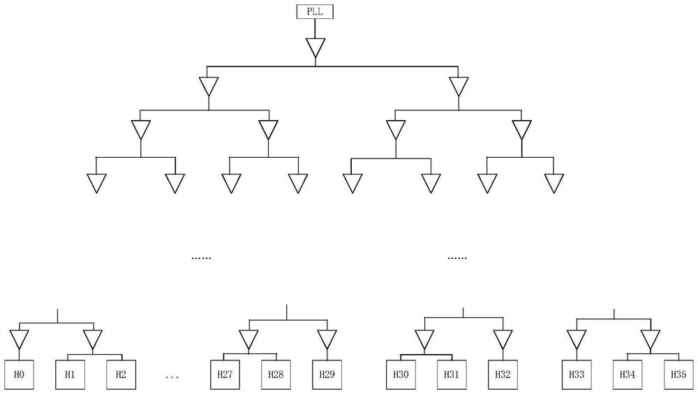
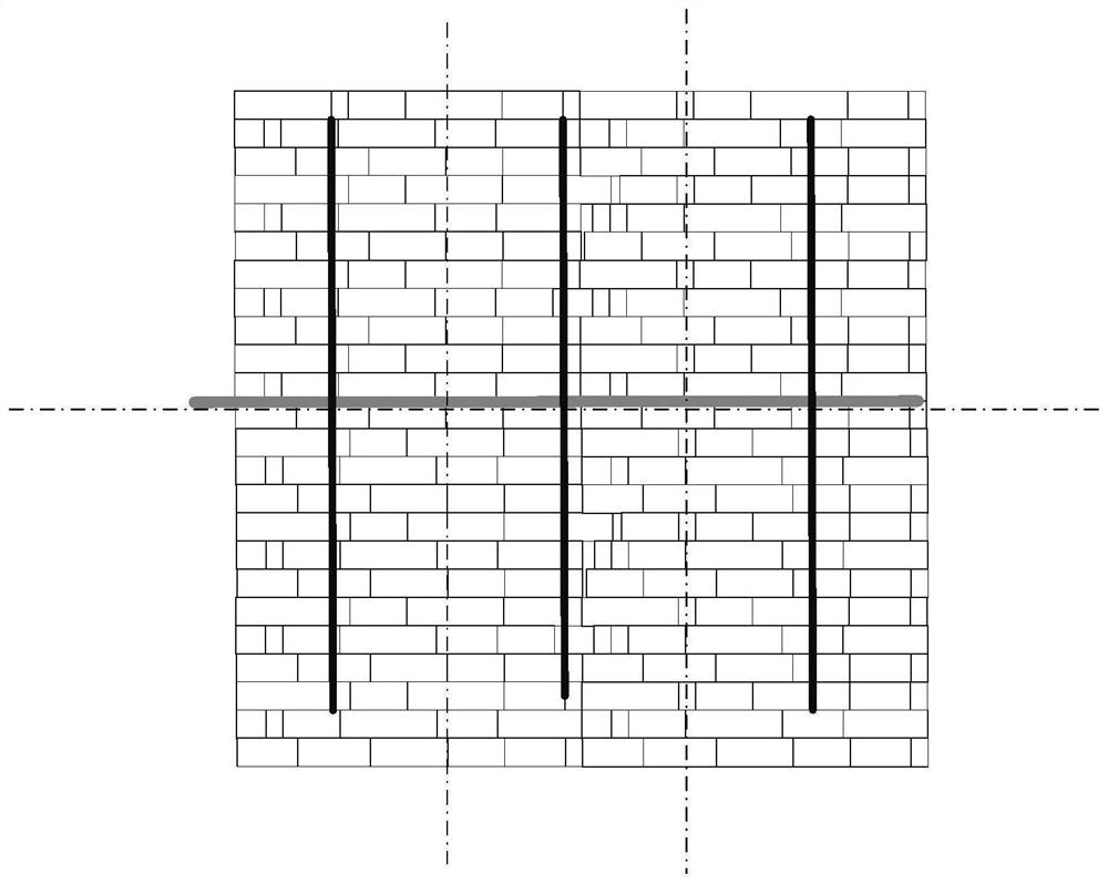
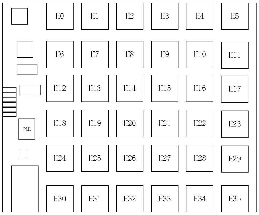
[0031] Refer to attached figure 2 , attached Figure 4 And attached Figure 5 , the present invention discloses a fishbone clock tree, comprising a main clock tree and several sub clock trees, the main clock tree is derived from the PLL, the sub clock tree is derived from the main clock tree, and the sub clock tree is provided with A number of clock bifurcation points, the clock bifurcation point as the source of the traditional clock tree to establish the traditional clock tree.
[0032] In this embodiment, the main clock tree is arranged on the central axis of the chip. Set the main clock tree on the central axis of the chip or at the center of multiple sub-modules of the chip, so that the sub-modules of the chip are distributed as evenly as possible on both sides of the main clock tree, which can reduce the length of wiring and wiring from the physical distance. quantity. At the same time, when the main clock tree is located on the central axis of the chip, the sub-clo...
Embodiment 2
[0039] The present invention also discloses a method for realizing a fishbone clock tree. Applying the fishbone clock tree in Embodiment 1 to a chip mainly includes the following steps:
[0040] Step 1. Obtain the sub-module layout of the chip.
[0041] Step 2. Lead the main clock tree from the PLL of the chip and set the main clock tree according to the sub-module layout so that the main clock tree is located on the central axis of the chip.
[0042] Step 3. Lead out several sub-clock trees from the main clock tree, and make the sub-clock trees evenly distributed on both sides of the main clock tree.
[0043] Step 4. A clock bifurcation point is derived from the sub-clock tree, and a traditional clock tree is established using the clock bifurcation point as the source of the traditional clock tree.
[0044] In step 1, since different chips have different numbers of sub-modules during design, and the arrangement positions of these sub-modules are also different, so when apply...
Embodiment 3
[0053] On the basis of embodiment 2, with reference to the attached figure 2 , when the chip is laid out as a single-layer sub-module, the sub-clock tree derived from the main clock tree divides the chip into several sub-regions, and a traditional clock tree is established in each sub-region through the clock bifurcation points derived from the sub-clock tree.
PUM
 Abstract
Description
Claims
Application Information


