Micro LED display panel and preparation method thereof

A technology for display panels and glass substrates, applied in electrical components, electric solid devices, circuits, etc., can solve problems such as uneven brightness of display panels, lower voltage difference of light-emitting devices, etc., to reduce the distance between VDD and VSS in the plane, Improved voltage drop and low resistance effects

Active Publication Date: 2021-12-03
SHENZHEN CHINA STAR OPTOELECTRONICS SEMICON DISPLAY TECH CO LTD
View PDF4 Cites 2 Cited by
  • Summary
  • Abstract
  • Description
  • Claims
  • Application Information

AI Technical Summary

Problems solved by technology

[0005] The purpose of the present invention is to provide a Micro LED display panel and its preparation method to solve the problem of uneven brightness of the display panel due to the voltage drop of VDD and the voltage rise of VSS caused by wiring resistance and the decrease of the voltage difference between the two ends of the light-emitting device. question

Method used


Image

  • Micro LED display panel and preparation method thereof
  • Micro LED display panel and preparation method thereof
  • Micro LED display panel and preparation method thereof

Examples


Embodiment Construction

[0044]The technical solutions in the embodiments of the present application will be clearly and completely described below in conjunction with the drawings in the embodiments of the present application. In the description of the present application, it should be understood that the terms "first" and "second" are used for description purposes only, and cannot be interpreted as indicating or implying relative importance or implicitly indicating the quantity of indicated technical features. Thus, a feature defined as "first" or "second" may explicitly or implicitly include one or more of said features. In the description of the present application, "plurality" means two or more, unless otherwise specifically defined.

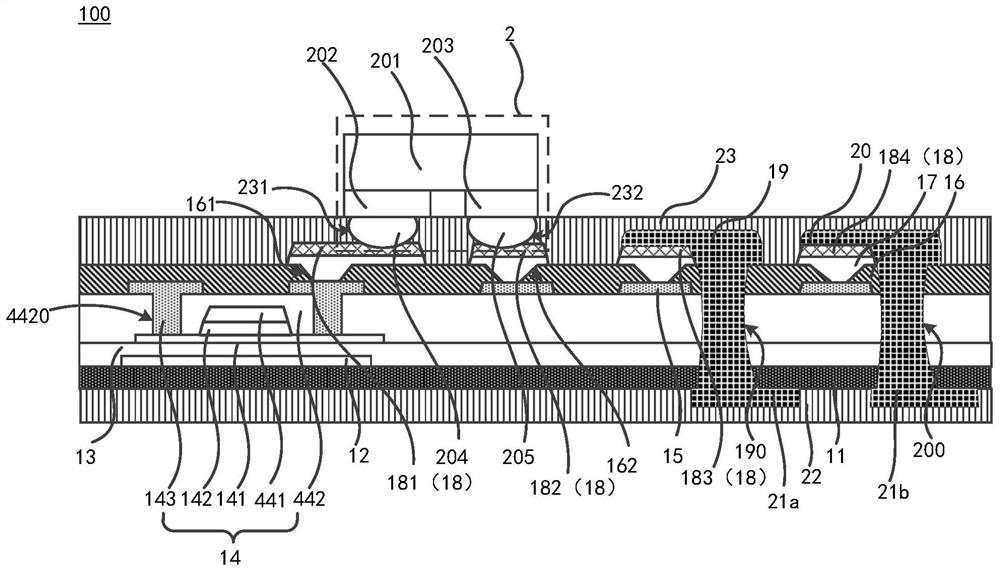
[0045] Such as figure 1 As shown, this embodiment provides a Micro LED display panel 100, including an array substrate 1, the array substrate 1 includes a glass substrate 11, a light shielding layer 12, a buffer layer 13, a thin film transistor layer 14, an active...


PUM


Abstract

The invention discloses a Micro LED display panel and a preparation method thereof. The Micro LED display panel comprises a glass substrate, a shading layer, a buffer layer, a thin film transistor layer, a passivation layer, an ITO connecting layer, a common connecting layer, a first metal wire and a second metal wire, wherein the common connecting layer is arranged on the ITO connecting layer and is patterned to form a first electrode, a second electrode, a VDD wire and a VSS wire; a first metal through hole and a second metal through hole sequentially penetrate through the passivation layer, a dielectric layer, the buffer layer and the glass substrate; the first metal through hole is filled with the first metal wire, and the VDD wire is covered with the first metal wire; and the second metal through hole is filled with the second metal wire, and the VSS wire is covered with the second metal wire. According to the Micro LED display panel, a punching mode is adopted, so that the VDD wire and the VSS wire which are located on the front face of the array substrate are connected to a first metal connecting layer and a second metal connecting layer which are located on the back face of the array substrate, and due to the fact that display is not affected by the back face wire, low resistance is achieved by increasing the wire width and the film thickness of the back face wire.

Description

technical field [0001] The present application relates to the field of display technology, in particular to a Micro LED display panel and a preparation method thereof. Background technique [0002] Micro LED Display (Micro LED Display) is a new generation of display technology. Micro LED inherits the characteristics of LED, with small size, light weight, high brightness, long life, low power consumption, fast response time and controllability Strong advantages, and the color gamut of Micro LED can be greater than 120%, and the PPI (pixel density) can reach 1500. Therefore, many panel manufacturers are participating in the development of Micro LED technology. [0003] However, micro light-emitting diode displays still have many technical difficulties to be overcome. For example, in the area far away from the VDD / VSS input terminal on a large-scale display, the voltage drop of VDD and the voltage rise of VSS due to the wiring resistance will cause voltage across the LED chip....

Claims


Application Information

Patent Timeline
Patent Type & Authority Applications(China)
IPC IPC(8): H01L27/15H01L33/62
CPCH01L27/15H01L33/62H01L2933/0066
Inventor 刘念卢马才
Owner SHENZHEN CHINA STAR OPTOELECTRONICS SEMICON DISPLAY TECH CO LTD
Why Eureka
Try Eureka