Check patentability & draft patents in minutes with Patsnap Eureka AI!

Soldering method for electric connection between mother board and electronic elements

A technology of electronic components and welding methods, which is applied in the field of welding where the main board and electronic components are electrically combined, can solve the problems of poor flatness of the welding surface, poor reliability, and low productivity, and achieve good coplanarity and improved reliability. , the effect of improving productivity

Inactive Publication Date: 2004-02-04
FOXCONN (KUNSHAN) COMPUTER CONNECTOR CO LTD +1
View PDF0 Cites 0 Cited by
  • Summary
  • Abstract
  • Description
  • Claims
  • Application Information

AI Technical Summary

Problems solved by technology

However, if figure 1 As shown, in the prior art, when the motherboard 24 is electrically combined with the electrical connector or the chip package 10, usually after the solder balls 14 are implanted on the soldering surface of the electrical connector or the chip package 10, the solder balls 14 are directly planted on the soldering surface of the chip package 10. The electrical connector of the ball 14 or the chip package 10 and the motherboard 24 are surface-adhesively welded, so that the flatness of the soldering surface is poor due to the uneven size of the implanted solder ball 14 (eg figure 1 shown in the middle), resulting in poor reliability of soldering with the motherboard (such as figure 1 Shown below), resulting in an increase in the defect rate, and in serious cases, it is necessary to rework and replace components, resulting in low productivity and waste of cost, and the finished product has a low life span and poor environmental resistance

Method used


Image

  • Soldering method for electric connection between mother board and electronic elements
  • Soldering method for electric connection between mother board and electronic elements
  • Soldering method for electric connection between mother board and electronic elements

Examples


Embodiment Construction

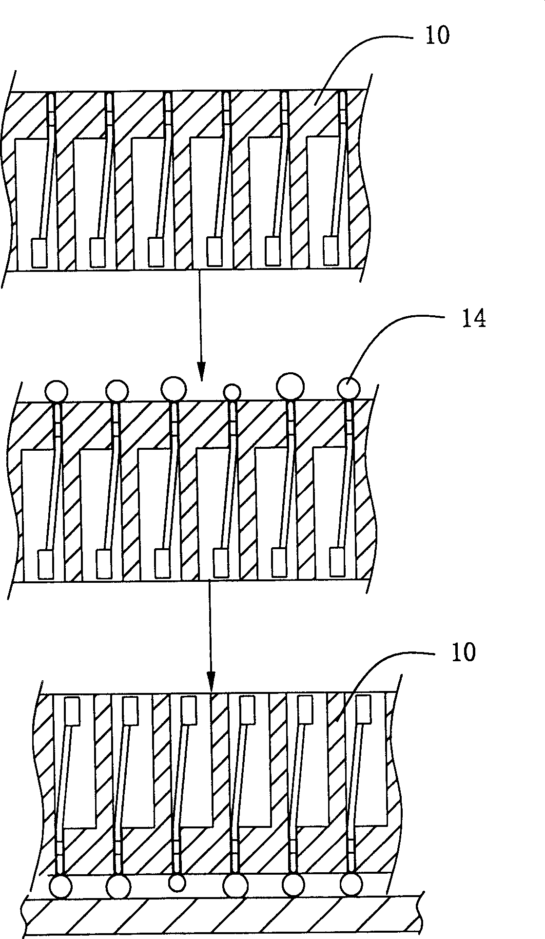
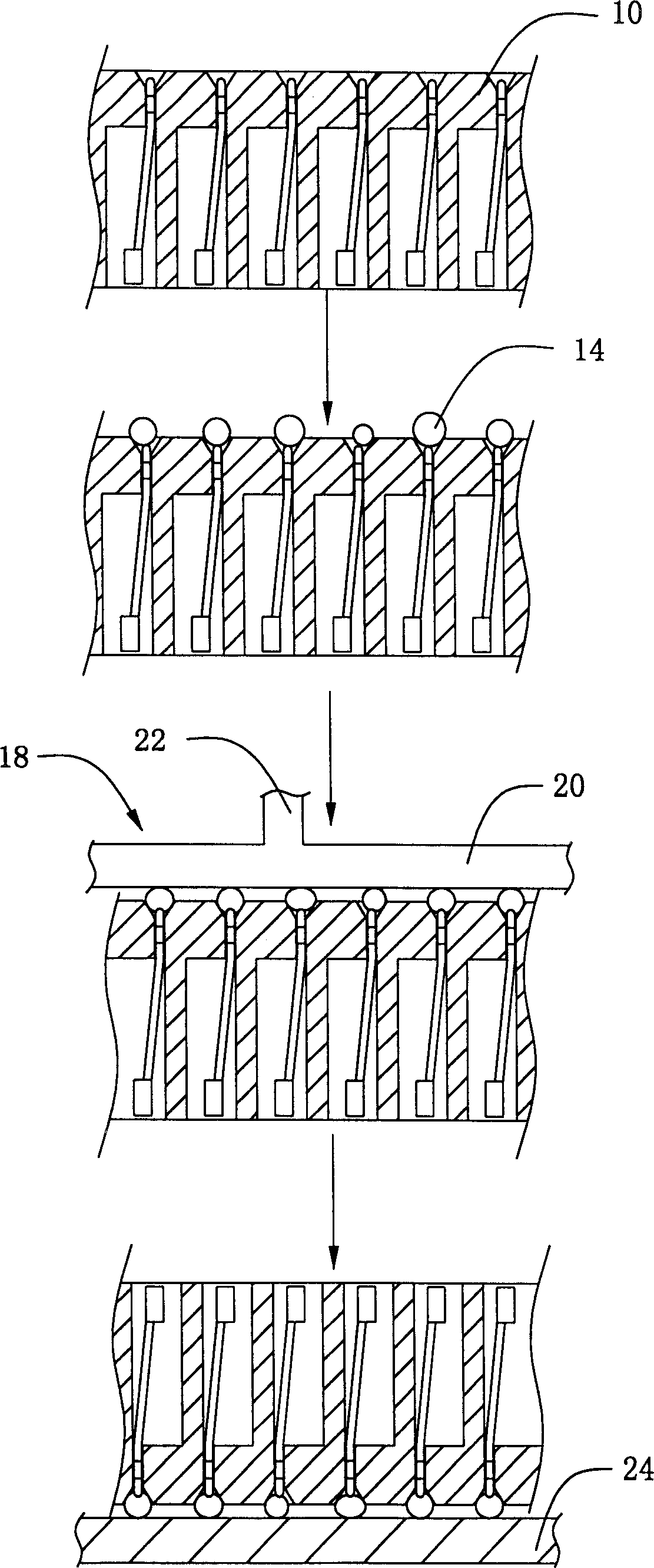
[0011] See figure 2 and image 3 It can be clearly seen that the steps of the present invention are as follows: step one is the pre-preparation process; step two is the solder ball planting process; step three is the flatness leveling process; step four is the welding process. Among them, the first step is to place the electronic component to be processed, such as the electrical connector or chip package 10, on the processing machine; the second step is to plant the solder ball 14 to one end of the conductive terminal 16 on the electrical connector or chip package 10 with a ball planting machine. ; Step three is to properly heat the solder ball 14 planted at one end of the conductive terminal 16 to a semi-molten state, and use the leveling tool 18 to add a pressure leveling step to it, the key part of the leveling tool 18 is a screed plate 20. The surface of the screed plate 20 in contact with the solder balls 14 has a high flatness; Step 4 is to flatten the electrical connector ...


PUM


Abstract

A soldering method for electric connection between mother board and electronic elements such as electric connector or IC package includes such steps as putting the electronic elements to be soldered on machine, transplanting soldering balls to one and of conducting terminals on electronic element by ball-transplanting machine, heating the soldering balls to semi-molten state, leveling the surfaces of soldering balls, aligning each leveled soldering balls to the connection points on mother board, and heating the soldering balls until they are molten.

Description

【Technical Field】 [0001] The present invention refers to a welding method for electrically combining a motherboard and an electronic component, in particular to a welding method for welding an electrical connector or chip package on the motherboard with good reliability. 【Background technique】 [0002] Welding connection methods are often used to connect motherboards and electronic components. Welding connections include surface bonding technology and through-hole welding technology. The through-hole welding technology requires a through-hole structure, which is not conducive to the wiring in the motherboard. However, the surface bonding technology does not require a through-hole structure, which greatly facilitates the layout of the lines in the motherboard and effectively utilizes the space on the motherboard. However, such as figure 1 As shown, in the prior art, when the motherboard 24 is electrically combined with the electrical connector or chip package 10, the solder balls...

Claims


Application Information

Patent Timeline
IPC IPC(8): H05K3/34
Inventor 林南宏刘政勋
Owner FOXCONN (KUNSHAN) COMPUTER CONNECTOR CO LTD
Features
  • R&D
  • Intellectual Property
  • Life Sciences
  • Materials
  • Tech Scout
  • Unparalleled Data Quality
  • Higher Quality Content
  • 60% Fewer Hallucinations
Learn More