Preparation method of fin type semiconductor device

A semiconductor and device technology, applied in the field of preparation of fin semiconductor devices, can solve the problems of poor flatness, affecting the working speed of the device, height difference, etc.

Active Publication Date: 2021-12-07
SHANGHAI INTEGRATED CIRCUIT EQUIP & MATERIALS IND INNOVATION CENT CO +1
View PDF5 Cites 0 Cited by
  • Summary
  • Abstract
  • Description
  • Claims
  • Application Information

AI Technical Summary

Problems solved by technology

With the continuous reduction of device size, in order to improve the carrier mobility in the fin field effect transistor and improve the performance of the transistor, generally the PMOS transistor in the fin field effect transistor will use silicon germanium to form fins to improve The carrier mobility of the PMOS tube, while the NMOS tube still uses silicon to form fins, and silicon and silicon germanium are located in diffe

Method used


Image

  • Preparation method of fin type semiconductor device
  • Preparation method of fin type semiconductor device
  • Preparation method of fin type semiconductor device

Examples


preparation example Construction

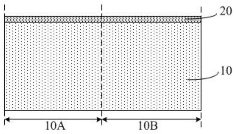
[0027] figure 1 A flow chart of the preparation method of the fin semiconductor device provided in this embodiment. This embodiment provides a method of preparing a fin semiconductor device to reduce the height difference of fins of the NMOS tube and the fins of the PMOS tube. Please refer to figure 1 The preparation method of the fins-type semiconductor device includes:

[0028] Step S1: Provides a substrate including a PMOS region and an NMOS region, the PMOS area for forming a PMOS tube, the NMOS region for forming an NMOS tube;

[0029] Step S2: Erochor to remove part of the substrate of the PMOS region;

[0030] Step S3: The fin material layer is protected on the substrate of the PMOS region and the NMOS region;

[0031] Step S4: The first mask layer and the second mask layer are sequentially formed on the fin material layer;

[0032] Step S5: The second mask layer of the partial thickness is removed by the first mask layer as a ground stop layer.

[0033] Step S6: Eroching ...


PUM


Abstract

The invention provides a fin-type semiconductor device preparation method, and the method comprises the steps: providing a substrate which comprises a PMOS region and an NMOS region; etching to remove partial thickness of the substrate in the PMOS region; forming a fin material layer on the substrate in the PMOS region and the NMOS region in a shape-preserving manner; sequentially forming a first mask layer and a second mask layer on the fin material layer in a conformal manner; carrying out grinding to remove a part of thickness of the second mask layer; carrying out the etching to remove the first mask layer, the second mask layer, the fin material layer of the NMOS region and the fin material layer of partial thickness of the PMOS region; forming a fin of the NMOS tube in the NMOS region, and forming a fin of the PMOS tube in the PMOS region. According to the invention, the height difference between the fins of the NMOS transistor and the fins of the PMOS transistor is reduced.

Description

Technical field [0001] The present invention relates to the field of semiconductor technology, and more particularly to a method of preparing a fin semiconductor device. Background technique [0002] Fin Field Effect Transistor, FINFET is a complementary metal oxidation semiconductor field effect transistor, including a vertical type channel structure, also known as fins, fins on both sides of the fin, FinFET structure Make more devices, higher performance, and fins-type semiconductor devices have been widely used in the field of memory and logic devices. As the size of the device is constantly reduced, in order to improve the carrier mobility in the fin field effect transistor, the performance of the transistor is improved, and the PMOS tube in the general fin field effect transistor will use germanic silicon to form fin to improve. The mobility of the carrier of the PMOS tube, while the NMOS tube still uses silicon to form fin, while silicon and silicon are located in different...

Claims


Application Information

Patent Timeline
IPC IPC(8): H01L21/8234
CPCH01L21/823431H01L21/823412Y02P70/50
Inventor 耿金鹏刘洋杨渝书
Owner SHANGHAI INTEGRATED CIRCUIT EQUIP & MATERIALS IND INNOVATION CENT CO
Why Eureka
Try Eureka