Optical integrated packaging semiconductor light source device

An optical integration and semiconductor technology, applied in the direction of semiconductor devices, electrical components, circuits, etc., can solve the problems of low light extraction efficiency and accelerated aging of devices due to overheating, and achieve the goals of reducing calorific value, delaying aging rate, and increasing light extraction efficiency Effect

Pending Publication Date: 2021-12-07
深圳瑞识智能科技有限公司
View PDF0 Cites 0 Cited by
  • Summary
  • Abstract
  • Description
  • Claims
  • Application Information

AI Technical Summary

Problems solved by technology

[0004] Based on this, it is necessary to provide an optically integrated packaged semiconductor light source device with high light extraction efficiency and low heat generation for the technical problems of low light extraction efficiency and accelerated aging of the device.

Method used


Image

  • Optical integrated packaging semiconductor light source device
  • Optical integrated packaging semiconductor light source device

Examples


Embodiment Construction

[0018] In order to make the above objects, features and advantages of the present invention more comprehensible, specific implementations of the present invention will be described in detail below in conjunction with the accompanying drawings. In the following description, numerous specific details are set forth in order to provide a thorough understanding of the present invention. However, the present invention can be implemented in many other ways different from those described here, and those skilled in the art can make similar improvements without departing from the connotation of the present invention, so the present invention is not limited by the specific embodiments disclosed below.

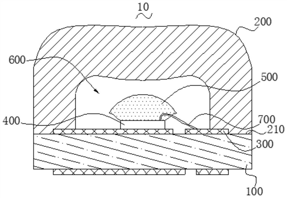
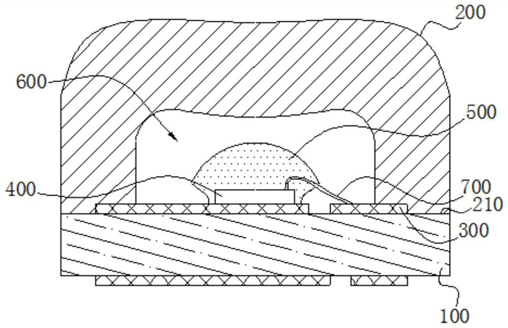
[0019] see figure 1 , the present invention provides an optically integrated packaged semiconductor light source device 10, which includes a substrate 100 provided with a circuit 300, an optical lens 200, an LED chip 400, and a light-transmitting adhesive layer 500, the optical lens 200 i...


PUM

PropertyMeasurementUnit
refractive indexaaaaaaaaaa

Abstract

The invention relates to the technical field of optical integrated devices, and particularly discloses an optical integrated packaging semiconductor light source device which is higher in light extraction efficiency and lower in device calorific value. The optical integrated packaging semiconductor light source device comprises a substrate, an optical lens, an LED chip and a light-transmitting glue layer, the substrate is provided with a circuit, and the optical lens is fixedly connected with the substrate. A light source cavity is arranged between the optical lens and the substrate, the LED chip and the light-transmitting glue layer are respectively accommodated in the light source cavity, and the LED chip is arranged at the top of the circuit and is electrically connected with the circuit; the light-transmitting glue layer is at least arranged on the upper surface of the LED chip, and the light-transmitting glue layer is used for reducing the Fresnel loss when the light of the LED chip is taken out; the outer surface of the light-transmitting glue layer is a convex cambered surface, and the convex cambered surface is used for reducing the total reflection loss of the light emitted by the LED chip.

Description

technical field [0001] The invention relates to the technical field of optical integrated devices, in particular to an optical integrated packaging semiconductor light source device. Background technique [0002] LED is a lighting device that integrates many advantages such as small size, low power consumption, high brightness, environmental protection, durability and long service life. In order to improve the light spot quality of the product and at the same time make the product both thinner and smaller, some packaging factories have combined the secondary lens with the LED chip. Specifically, by designing a smaller lens above the LED chip The optical lens uses the refraction of light by the optical lens to adjust the shape of the spot generated by the LED chip and improve the quality of the spot. That is to say, the function of the lens is integrated into the LED chip to complete the chip-level optical lens design. [0003] However, in traditional optical lens-type light...

Claims


Application Information

Patent Timeline
Patent Type & Authority Applications(China)
IPC IPC(8): H01L33/54H01L33/58H01L33/64H01L33/62
CPCH01L33/58H01L33/642H01L33/54H01L33/62H01L33/50H01L2933/0091H01L33/0095H01L33/505
Inventor 黄伟曹宇星汪洋
Owner 深圳瑞识智能科技有限公司
Why Eureka
Try Eureka