A kind of pcb solder mask window opening automatic processing method

A technology of automatic processing and window opening, which is used in electrical digital data processing, special data processing applications, CAD circuit design, etc. Problems such as poor efficiency, to avoid the tombstone effect, avoid the size of the tin receiving area, and ensure the effect of the yield

Active Publication Date: 2022-05-10
HUIZHOU KING BROTHER CIRCUIT TECH
View PDF0 Cites 0 Cited by
  • Summary
  • Abstract
  • Description
  • Claims
  • Application Information

AI Technical Summary

Problems solved by technology

The effect of solder mask window opening is related to the quality of subsequent electronic component soldering, so it needs to be optimized when solder mask window opening. In traditional operations, most of them only optimize the solder mask at the BGA, and the BGA needs to be manually defined. Attributes, optimization takes a long time, CAM processing efficiency is poor, often produces tombstone effect (tombstone effect refers to the physical board at the connection between the pad and the wire, and it will be biased towards the position of the wire when soldering, causing the shape of the pad to deform and resulting in uneven soldering Phenomenon that affects soldering performance), and the size of the solder mask window is difficult to keep consistent, resulting in different sizes of soldered pads

Method used


Image

  • A kind of pcb solder mask window opening automatic processing method
  • A kind of pcb solder mask window opening automatic processing method
  • A kind of pcb solder mask window opening automatic processing method

Examples


Embodiment Construction

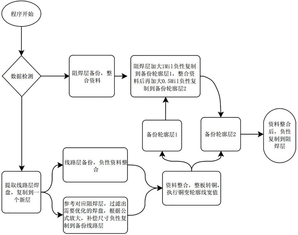
[0031] In order to facilitate those skilled in the art to understand the present invention, the present invention will be further described in detail below in conjunction with specific embodiments and accompanying drawings.

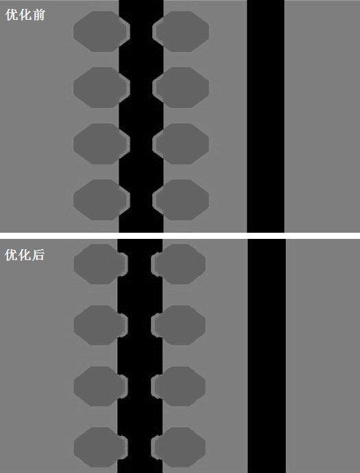
[0032] refer to Figure 1 to Figure 6 , the present invention provides an automatic processing method for PCB solder resist window opening, comprising: checking and extracting the data of both the circuit layer and the solder resist layer, and duplicating and backing up the data of the two, and screening out the solder that needs to be optimized according to the data. Disk, copy the data of the pads that need to be optimized in the circuit layer to the backup of the circuit layer data, and integrate the positive and negative data to obtain the backup contour layer, optimize the data of the backup contour layer, and save the optimized The backup contour layer and the backup of the solder mask layer are negatively superimposed to complete the solder mask op...


PUM


Abstract

The present invention relates to the technical field of PCB, in particular to an automatic processing method for PCB solder mask window opening, which checks and extracts the data of both the circuit layer and the solder mask layer, and copies and backs up the data of both, and screens out the data that needs to be optimized according to the data. pads, copy the data of the pads that need to be optimized in the circuit layer to the backup of the circuit layer data, and integrate the positive and negative data to obtain the backup contour layer, optimize the data of the backup contour layer, and optimize The final backup contour layer and the backup of the solder mask layer are negatively superimposed to complete the solder mask optimization. The invention can quickly and automatically process the solder mask opening of the PCB, improve the CMA processing efficiency, automatically optimize the solder mask during the process, avoid the tombstone effect, improve the quality of the product, and ensure the yield rate. The invention can ensure the consistency of the size of the solder-resisting window of the same kind of pads, make the shape of the solder joints more beautiful, and avoid the problem of different sizes of tin-receiving areas of the pads.

Description

technical field [0001] The invention relates to the technical field of PCBs, in particular to an automatic processing method for soldering and window opening of PCBs. Background technique [0002] PCB (printed circuit board) is one of the important components of the electronics industry. Almost every kind of electronic equipment, ranging from electronic watches and calculators to computers, communication electronic equipment, and military weapon systems, as long as there are electronic components such as integrated circuits , In order to make the electrical interconnection between the various components, printed boards are used. Common circuit boards generally include single-sided boards, double-sided boards, and multi-layer boards. Solder mask opening means that the copper skin is exposed on the solder mask layer of the PCB where it needs to be soldered, that is, the ink is not covered at this position, so as to facilitate the subsequent connection of electronic components...

Claims


Application Information

Patent Timeline
Patent Type & Authority Patents(China)
IPC IPC(8): G06F30/398G06F30/3953G06F115/12
CPCG06F30/398G06F30/3953G06F2115/12
Inventor 张仪宗谭林黄双双历振铎胡容刚田晓燕
Owner HUIZHOU KING BROTHER CIRCUIT TECH
Why Eureka
Try Eureka