Gallium nitride epitaxial wafer and growth method thereof

A growth method, gallium nitride technology, applied in the field of growth of gallium nitride epitaxial wafers and their epitaxial wafers, can solve the problems of poor quality of gallium nitride epitaxial wafers, achieve shortened production time, good crystal quality, and reduce dislocations effect of density

Active Publication Date: 2021-12-21
JIANGSU INST OF ADVANCED SEMICON CO LTD
View PDF2 Cites 1 Cited by
  • Summary
  • Abstract
  • Description
  • Claims
  • Application Information

AI Technical Summary

Problems solved by technology

[0004] The purpose of the present invention is to provide a gallium nitride epitaxial wafer and a method for growing the epitaxial wafer, which has solved the problem of low quality of the gallium nitride epitaxial wafer prepared by only one layer of buffer layer in the prior art

Method used


Image

  • Gallium nitride epitaxial wafer and growth method thereof
  • Gallium nitride epitaxial wafer and growth method thereof
  • Gallium nitride epitaxial wafer and growth method thereof

Examples


Embodiment Construction

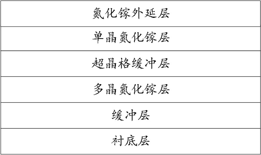
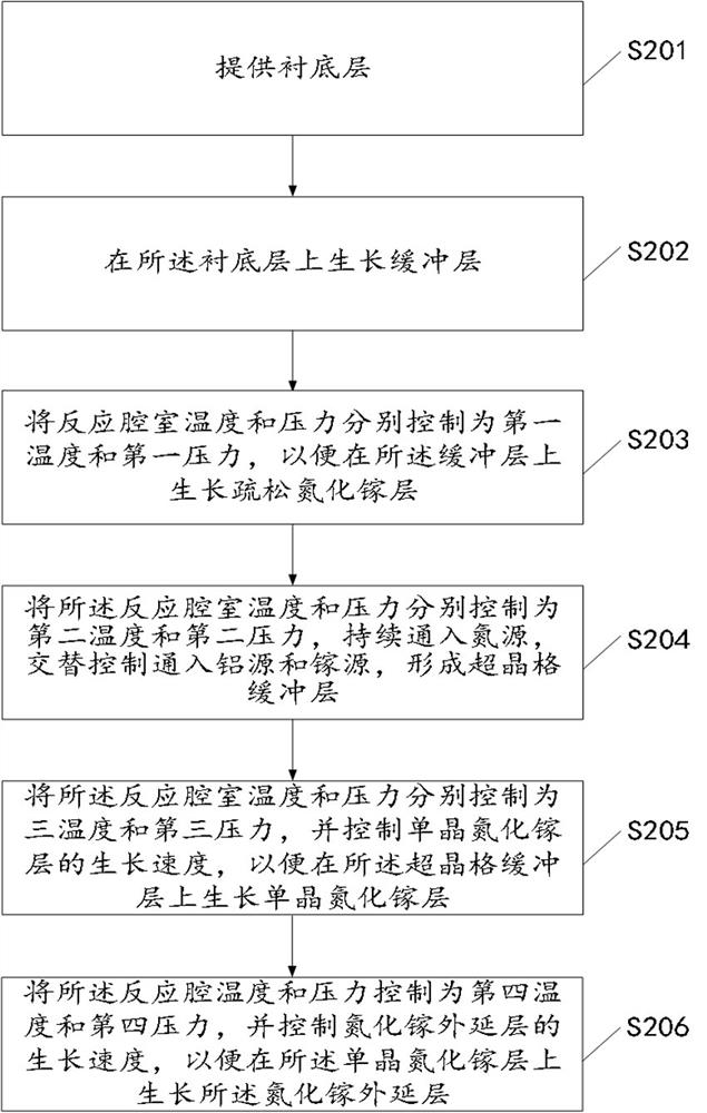
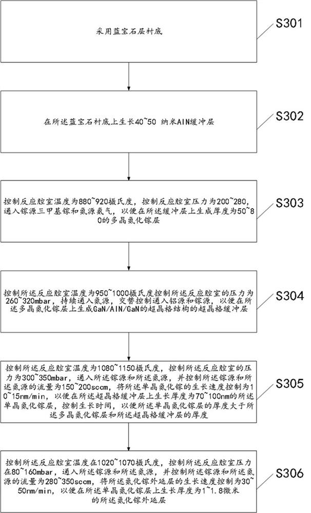
[0044] The core of the present invention is to provide a gallium nitride epitaxial wafer and a method for growing the epitaxial wafer, increase the polycrystalline gallium nitride layer to buffer the stress, the superlattice buffer layer further buffer the stress, improve the crystal quality, and the single crystal gallium nitride layer Improve the quality of GaN epitaxial wafers, reduce dislocation density, and finally form high-quality GaN epitaxial wafers.

[0045] In order to enable those skilled in the art to better understand the solution of the present invention, the present invention will be further described in detail below in conjunction with the accompanying drawings and specific embodiments. Apparently, the described embodiments are only some of the embodiments of the present invention, but not all of them. Based on the embodiments of the present invention, all other embodiments obtained by persons of ordinary skill in the art without making creative efforts belong...


PUM

PropertyMeasurementUnit
thicknessaaaaaaaaaa
thicknessaaaaaaaaaa
thicknessaaaaaaaaaa

Abstract

The invention discloses a gallium nitride epitaxial wafer and a growth method thereof. The gallium nitride epitaxial wafer comprises a substrate layer, a buffer layer, a polycrystalline gallium nitride layer, a superlattice buffer layer, a single crystal gallium nitride layer and a gallium nitride epitaxial wafer, sapphire serves as the substrate layer, the buffer layer grows on the substrate layer, the polycrystalline gallium nitride layer grows on the buffer layer, and the single crystal gallium nitride layer grows on the single crystal gallium nitride layer. A superlattice buffer layer grows on the polycrystalline gallium nitride layer, the single crystal gallium nitride layer grows on the superlattice buffer layer, the thickness of the single crystal gallium nitride layer is larger than the thickness of the polycrystalline gallium nitride layer and the thickness of the superlattice buffer layer, and finally a gallium nitride epitaxial layer grows on the single crystal gallium nitride layer. The buffer layer and the polycrystalline gallium nitride layer are adopted to release stress generated by lattice mismatch, the superlattice buffer layer not only can buffer the stress, but also can improve the lattice quality, and the monocrystal gallium nitride layer can improve the quality of the gallium nitride epitaxial wafer and reduce the dislocation density, so that the high-quality gallium nitride epitaxial layer is formed.

Description

technical field [0001] The invention relates to the field of semiconductors, in particular to a gallium nitride epitaxial wafer and a method for growing the epitaxial wafer. Background technique [0002] As the preparation of gallium nitride epitaxial wafers mainly relies on the epitaxial growth of gallium nitride from sapphire, while the existing epitaxial wafers are formed on sapphire substrates, although a buffer layer is formed, it can buffer the epitaxial wafers and the substrate. However, due to the lattice mismatch between GaN and sapphire substrates, a huge compressive stress is generated, and the stress cannot be fully buffered only through a buffer layer, and the existence of stress will cause warping of the epitaxial wafer. On the other hand, the single buffer layer of AlN or AlGaN makes the crystal quality of GaN not high, and the structure of the epitaxial wafer needs to be further optimized to form a high-quality epitaxial wafer structure. [0003] In summary,...

Claims


Application Information

Patent Timeline
Patent Type & Authority Applications(China)
IPC IPC(8): C30B29/68C30B25/18C30B25/20C30B28/14C30B29/40
CPCC30B29/68C30B29/406C30B29/403C30B25/183C30B25/20C30B28/14
Inventor 李利哲王国斌
Owner JIANGSU INST OF ADVANCED SEMICON CO LTD
Why Eureka
Try Eureka