An automatic liquid level compensation method

A technology of automatic compensation and liquid level, applied in chemical instruments and methods, self-melting liquid pulling method, single crystal growth, etc., can solve the problems of inaccurate control accuracy and inability to form a whole rod, so as to improve the yield and effectively Favorable effect on crystal growth

Active Publication Date: 2022-07-26
浙江晶阳机电股份有限公司
View PDF0 Cites 0 Cited by
  • Summary
  • Abstract
  • Description
  • Claims
  • Application Information

AI Technical Summary

Problems solved by technology

[0003] In the production process, the accurate control of the liquid port distance is a very important factor affecting the production of monocrystalline silicon. In the prior art, the liquid port distance control in the production process is indirectly controlled by the weight change of the monocrystalline silicon product The change of the gap distance has the defect of inaccurate control accuracy, which leads to the ingot being broken during the production process and unable to form a whole rod

Method used


Image

  • An automatic liquid level compensation method
  • An automatic liquid level compensation method
  • An automatic liquid level compensation method

Examples


Embodiment 1

[0029] A liquid level automatic compensation method, comprising the following steps:

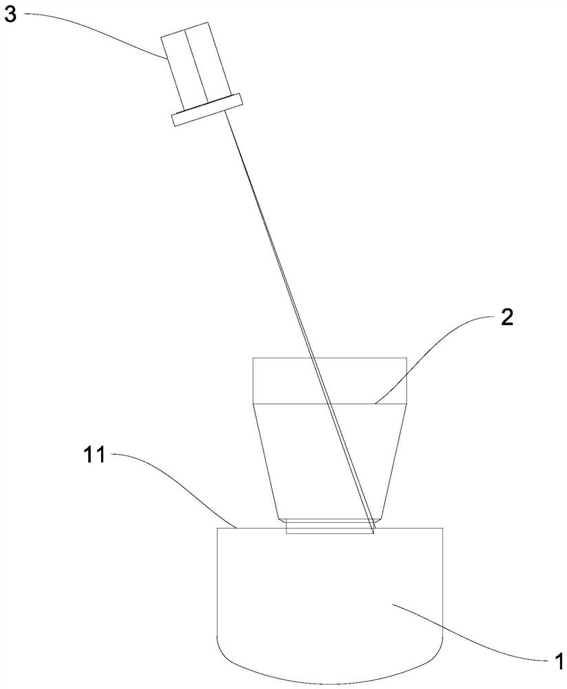
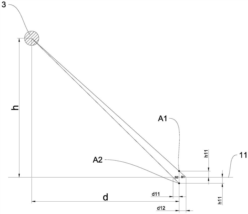
[0030] S1: The crucible 1 contains silicon liquid, the crucible 1 is provided with a water-cooled heat screen 2 above the silicon liquid level 11, an imaging device 3 is provided above the water-cooled heat screen 2, and a lift is provided below the crucible 1 device 5;

[0031] S2: The imaging device 3 emits light through the screen of the water-cooled heat screen 2 to form an observation point A1 on the silicon liquid level 11, and the observation point A1 forms an observation line-B1 with a length of d12 on the silicon liquid level 11 At the same time, the screen mouth of the water-cooled and hot screen 2 forms a projection point A2 under the mirror projection of the silicon liquid level 11, and the projection point A2 forms an observation line B2 with a length of d11 on the silicon liquid level 11. The imaging device 3 is far from the silicon liquid level 11. The distance between the li...

Embodiment 2

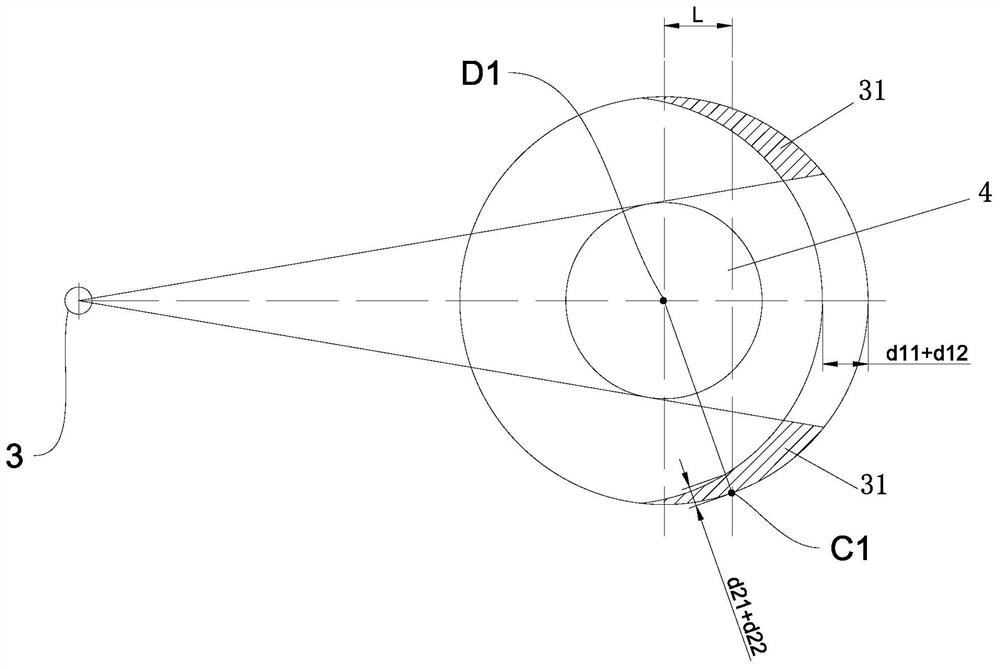
[0040] The screen mouth of the water-cooled and hot screen 2 is in the shape of a crescent when the imaging device 3 is imaging. In the actual production process, the raw materials are melted and then crystallized to form a crystal rod. Therefore, the visible area of ​​the actual imaging device 3 is as follows: image 3 shown. In the actual imaging area, the measurement position of d11+d12 cannot be directly selected for measurement due to the position of the ingot 4. Therefore, in the actual use process, in the middle area of ​​the imaging visible area 31, take an observation point three C1, the observation point The horizontal distance between C1 and the imaging center is L, and the distance d21+d22 that needs to be measured is obtained by connecting the line with the imaging center.

[0041] In the step S2, the light emitted by the imaging device 3 is imaged as the imaging visible area 31 through the water-cooling and hot screen 2, the center of the imaging visible area 31 ...


PUM


Abstract

The invention relates to the technical field of monocrystalline silicon production, and relates to an automatic liquid level compensation method. The invention includes: S1: a crucible is filled with silicon liquid, and a water cooling and heating screen is arranged above the liquid level of the silicon liquid in the crucible. An imaging device is arranged above the cooling and heating screen, and a lifting device is arranged below the crucible; S2: The imaging device emits light through the screen of the water-cooling and heating screen to form an observation point 1 on the liquid silicon liquid surface, and the observation point 1 is on the liquid silicon liquid. Observation line 1 is formed on the liquid surface, and at the same time, the screen opening of the water-cooled and hot screen forms a projection point under the mirror projection of the silicon liquid surface, and the projection point forms an observation line 2 on the silicon liquid surface. The distance between the imaging device and the silicon liquid surface is h, and the distance between the imaging device and the screen of the water-cooled heat screen is d, which satisfies: d11 / h11=d / (h+h11), d12 / h11=d / (h‑h11); S3: According to step S2 The formula solves the value of the liquid port distance h11. S4: Compare the liquid port distance h11 solved in the step S3 with the preset optimal liquid level position, and use the lifting device to compensate for the lifting according to the comparison result, so that the adjustment is accurate and the operation is simple.

Description

technical field [0001] The invention relates to the technical field of monocrystalline silicon production, and relates to an automatic liquid level compensation method. Background technique [0002] In the process of using a single crystal furnace to produce single crystal silicon, the liquid port distance refers to the distance between the liquid level of the raw material and the water cooling screen. It is a very important technical parameter in the production process of monocrystalline silicon, and monocrystalline silicon is the basic raw material in photovoltaic power generation and semiconductor industries. As a key supporting material for the modern information society, monocrystalline silicon is one of the most important monocrystalline materials in the world. It is not only the main functional material for the development of computers and integrated circuits, but also the main functional material for photovoltaic power generation and utilization of solar energy. [...

Claims


Application Information

Patent Timeline
Patent Type & Authority Patents(China)
IPC IPC(8): C30B29/06C30B15/26C30B15/30
CPCC30B29/06C30B15/26C30B15/30
Inventor 杨金海徐永根沈凯杰
Owner 浙江晶阳机电股份有限公司
Why Eureka
Try Eureka