Positive and negative voltage charge pump single-stage circuits and four-phase charge pump circuit
A four-phase charge pump, charge pump technology, applied in electrical components, conversion equipment without intermediate conversion to AC, output power conversion devices, etc., can solve the problem of high withstand voltage performance of the second PMOS tube PM2, and achieve withstand voltage Low requirements, reduced area, and guaranteed voltage conversion effect
- Summary
- Abstract
- Description
- Claims
- Application Information
AI Technical Summary
Problems solved by technology
Method used
Image

Examples
Embodiment 1
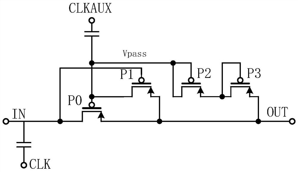
[0047] like image 3 As shown, the positive voltage charge pump single-stage circuit includes the zeroth PMOS transistor P0, the first PMOS transistor P1, the second PMOS transistor P2, the third PMOS transistor P3, the first capacitor C1 and the second capacitor C2;
[0048] The drain terminal of the zeroth PMOS transistor P0 and the gate terminal of the first PMOS transistor P1 are short-circuited as the voltage input terminal IN;
[0049] The gate end and the drain end of the third PMOS transistor P3 are short-circuited with the source end of the second PMOS transistor P2;
[0050] The source terminals of the zeroth PMOS transistor P0, the first PMOS transistor P1 and the third PMOS transistor P3 are short-circuited as the voltage output terminal OUT;
[0051] The voltage input terminal IN is connected to the main clock terminal CLK through the first capacitor C1;
[0052] After the gate terminal of the zeroth PMOS transistor P0 and the drain terminal of the first PMOS tran...
Embodiment 2
[0056] like Figure 4 As shown, the negative voltage charge pump single-stage circuit includes the zeroth NMOS transistor N0, the first NMOS transistor N1, the second NMOS transistor N2, the third NMOS transistor N3, the first capacitor C1 and the second capacitor C2;
[0057] The source terminal of the zeroth NMOS transistor N0 and the gate terminal of the first NMOS transistor N1 are short-circuited as the voltage input terminal IN;
[0058] The gate end and the source end of the third NMOS transistor N3 are short-circuited with the drain end of the second NMOS transistor N2;
[0059] The drain terminals of the zeroth NMOS transistor N0, the first NMOS transistor N1 and the third NMOS transistor N3 are short-circuited as the voltage output terminal OUT;
[0060] The voltage input terminal IN is connected to the main clock terminal CLK through the first capacitor C1;
[0061] After the gate terminal of the zeroth NMOS transistor N0 and the source terminal of the first NMOS ...
Embodiment 3
[0065] like Figure 5 As shown, a four-phase charge pump circuit comprising the charge pump single-stage circuit of Embodiment 1 or Embodiment 2 is formed by sequentially cascading four charge pump single-stage circuits;
[0066] The voltage output terminal OUT of the single-stage circuit of the previous charge pump is connected to the voltage input terminal IN of the single-stage circuit of the subsequent charge pump;
[0067] The voltage input terminal IN of the single-stage circuit of the first-stage charge pump is used as the input terminal VIN of the four-phase charge pump circuit;
[0068] The voltage output terminal OUT of the fourth-stage charge pump single-stage circuit is used as the output terminal VOUT of the four-phase charge pump circuit;
[0069] The first-phase clock PH1 is connected to the auxiliary clock terminal CLKAUX of the first-stage charge pump single-stage circuit and the third-stage charge pump single-stage circuit;
[0070] The second phase clock P...
PUM
 Abstract
Description
Claims
Application Information