Method, device and equipment for calculating wafer period in wafer
A computing method and technology in wafers, applied in computing, image data processing, instruments, etc., can solve problems such as slow computing speed and long time consumption, and achieve the effect of increasing speed and stability, increasing adaptability, and reducing manual intervention.
- Summary
- Abstract
- Description
- Claims
- Application Information
AI Technical Summary
Problems solved by technology
Method used
Image

Examples
Embodiment Construction
[0065] The present invention will be further described in detail below in conjunction with the accompanying drawings and embodiments. It should be understood that the specific embodiments described here are only used to explain the present invention, but not to limit the present invention. In addition, it should be noted that, for the convenience of description, only some structures related to the present invention are shown in the drawings but not all structures.
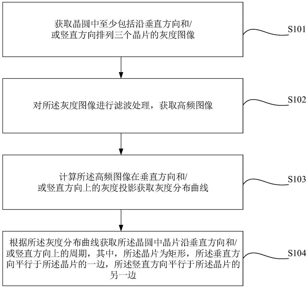
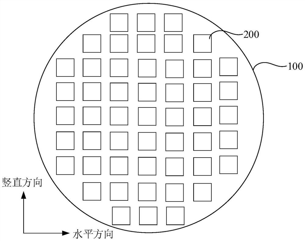
[0066] There are a plurality of dies arranged in an array on the wafer, and there are grooves between the dies, and the dies are generally rectangular. After the wafer is formed on the wafer, it is necessary to use machine vision to detect whether there is a defect in the wafer. At this time, it is necessary to set the robot arm of the machine vision according to the field of view of the machine vision, parameters such as resolution, and the period between wafers. movement path. In the prior art, the period betwe...
PUM
 Abstract
Description
Claims
Application Information